- 您现在的位置:买卖IC网 > PDF目录10296 > AD7450ABRM-REEL7 (Analog Devices Inc)IC ADC 12BIT W/DIFF INP 8-MSOP PDF资料下载
参数资料
| 型号: | AD7450ABRM-REEL7 |
| 厂商: | Analog Devices Inc |
| 文件页数: | 14/29页 |
| 文件大小: | 0K |
| 描述: | IC ADC 12BIT W/DIFF INP 8-MSOP |
| 标准包装: | 1,000 |
| 位数: | 12 |
| 采样率(每秒): | 1M |
| 数据接口: | DSP,MICROWIRE?,QSPI?,串行,SPI? |
| 转换器数目: | 1 |
| 功率耗散(最大): | 9.25mW |
| 电压电源: | 单电源 |
| 工作温度: | -40°C ~ 85°C |
| 安装类型: | 表面贴装 |
| 封装/外壳: | 8-TSSOP,8-MSOP(0.118",3.00mm 宽) |
| 供应商设备封装: | 8-MSOP |
| 包装: | 带卷 (TR) |
| 输入数目和类型: | 1 个差分,单极 |
| 配用: | EVAL-AD7450CBZ-ND - BOARD EVALUATION FOR AD7450 |
第1页第2页第3页第4页第5页第6页第7页第8页第9页第10页第11页第12页第13页当前第14页第15页第16页第17页第18页第19页第20页第21页第22页第23页第24页第25页第26页第27页第28页第29页
AD7440/AD7450A
Rev. C | Page 20 of 28
Example 1
Table 6. Examples of Suitable Voltage References
Output
Voltage (V)
Initial
Accuracy (%)
Operating
Current (μA)
VIN max = VDD + 0.3
VIN max = VREF + VREF/2
Reference
AD780
2.5/3
0.04
1000
If VDD = 5 V, then VIN max = 5.3 V.
Therefore
3 × VREF/2 = 5.3 V
VREF max = 3.5 V
Thus, when operating at VDD = 5 V, the value of VREF can range
from 100 mV to a maximum value of 3.5 V. When VDD = 4.75 V,
VREF max = 3.17 V.
Example 2
VIN max = VDD + 0.3
VIN max = VREF + VREF/2
If VDD = 3 V, then VIN max = 3.3 V.
Therefore,
3 × VREF/2 = 3.3 V
VREF max = 2.2 V
Thus, when operating at VDD = 3 V, the value of VREF can range
from 100 mV to a maximum value of 2.2 V. When VDD = 2.7 V,
VREF max = 2 V.
These examples show that the maximum reference applied to
the AD7440/AD7450A is directly dependent on the value
applied to VDD.
The value of the reference sets the analog input span and the
common-mode voltage range. Errors in the reference source
result in gain errors in the AD7440/AD7450A transfer function
and add to specified full-scale errors on the part. A 0.1 μF
capacitor should be used to decouple the VREF pin to GND.
Table 6 lists examples of suitable voltage references.
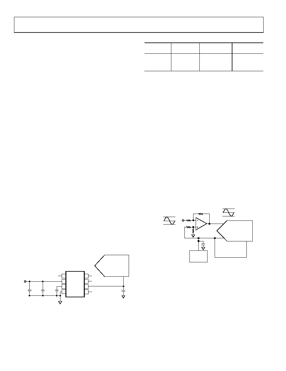
03051-A
-038
1
AD780
NC
8
2
VIN
NC
7
3
GND
6
4
TEMP
5
OPSEL
TRIM
VOUT
AD7440/
AD7450A*
VREF
2.5V
NC
VDD
NC
VDD
NC = NO CONNECT
10nF
0.1
μF
0.1
μF
0.1
μF
*ADDITIONAL PINS OMITTED FOR CLARITY
Figure 38. Typical VREF Connection Diagram for VDD = 5 V
ADR421
2.5
0.04
500
ADR420
2.048
0.05
500
SINGLE-ENDED OPERATION
When supplied with a 5 V power supply, the AD7440/AD7450A
can handle a single-ended input. The design of these devices is
optimized for differential operation, so with a single-ended
input, performance degrades. Linearity degrades by typically
0.2 LSB, the full-scale errors degrade typically by 1 LSB, and ac
performance is not guaranteed.
To operate the AD7440/AD7450A in single-ended mode, the
V
input is coupled to the signal source, while the V
IN+
IN–
input is
biased to the appropriate voltage corresponding to the midscale
code transition. This voltage is the common mode, which is a
fixed dc voltage (usually the reference). The VIN+ input swings
around this value and should have a voltage span of 2 × VREF to
make use of the full dynamic range of the part. The input signal
therefore has peak-to-peak values of common mode ±VREF. If
the analog input is unipolar, an op amp in a noninverting unity
gain configuration can be used to drive the VIN+ pin. The ADC
operates from a single supply, so it is necessary to level shift
ground-based bipolar signals to comply with the input
requirements. An op amp can be configured to rescale and level
shift the ground-based bipolar signal, so it is compatible with
the selected input range of the AD7440/AD7450A (Figure 39).
03051-A
-039
R
5V
2.5V
0V
+2.5V
0V
–2.5V
R
0.1
μF
R
AD7440/
AD7450A
VREF
VIN+
VIN–
VIN
EXTERNAL
VREF (2.5V)
Figure 39. Applying a Bipolar Single-Ended Input to the AD7440/AD7450A
相关PDF资料 |
PDF描述 |
|---|---|
| MS3100F20-29P | CONN RCPT 17POS WALL MNT W/PINS |
| D38999/26FG75AN | CONN HSG PLUG 4POS STRGHT PINS |
| D38999/26FG75PNLC | CONN HSG PLUG 4POS STRGHT PINS |
| VI-B4F-MW-S | CONVERTER MOD DC/DC 72V 100W |
| VI-2TZ-MV-S | CONVERTER MOD DC/DC 2V 60W |
相关代理商/技术参数 |
参数描述 |
|---|---|
| AD7450ABRMZ | 功能描述:IC ADC 12BIT DIFF IN 1MSPS 8MSOP RoHS:是 类别:集成电路 (IC) >> 数据采集 - 模数转换器 系列:- 其它有关文件:TSA1204 View All Specifications 标准包装:1 系列:- 位数:12 采样率(每秒):20M 数据接口:并联 转换器数目:2 功率耗散(最大):155mW 电压电源:模拟和数字 工作温度:-40°C ~ 85°C 安装类型:表面贴装 封装/外壳:48-TQFP 供应商设备封装:48-TQFP(7x7) 包装:Digi-Reel® 输入数目和类型:4 个单端,单极;2 个差分,单极 产品目录页面:1156 (CN2011-ZH PDF) 其它名称:497-5435-6 |
| AD7450ABRMZ2 | 制造商:AD 制造商全称:Analog Devices 功能描述:Differential Input, 1 MSPS ADCs in an 8-Lead SOT-23 |
| AD7450ABRT-R2 | 功能描述:IC ADC 12BIT W/DIFF INP SOT-23-8 RoHS:否 类别:集成电路 (IC) >> 数据采集 - 模数转换器 系列:- 产品培训模块:Lead (SnPb) Finish for COTS Obsolescence Mitigation Program 标准包装:2,500 系列:- 位数:12 采样率(每秒):3M 数据接口:- 转换器数目:- 功率耗散(最大):- 电压电源:- 工作温度:- 安装类型:表面贴装 封装/外壳:SOT-23-6 供应商设备封装:SOT-23-6 包装:带卷 (TR) 输入数目和类型:- |
| AD7450ABRT-REEL7 | 制造商:AD 制造商全称:Analog Devices 功能描述:Differential Input, 1 MSPS 10-Bit and 12-Bit ADCs in an 8-Lead SOT-23 |
| AD7450ABRTZ-REEL7 | 功能描述:IC ADC 12BIT DIFF 1MSPS SOT23-8 RoHS:是 类别:集成电路 (IC) >> 数据采集 - 模数转换器 系列:- 其它有关文件:TSA1204 View All Specifications 标准包装:1 系列:- 位数:12 采样率(每秒):20M 数据接口:并联 转换器数目:2 功率耗散(最大):155mW 电压电源:模拟和数字 工作温度:-40°C ~ 85°C 安装类型:表面贴装 封装/外壳:48-TQFP 供应商设备封装:48-TQFP(7x7) 包装:Digi-Reel® 输入数目和类型:4 个单端,单极;2 个差分,单极 产品目录页面:1156 (CN2011-ZH PDF) 其它名称:497-5435-6 |
发布紧急采购,3分钟左右您将得到回复。