- 您现在的位置:买卖IC网 > PDF目录10314 > AD7450ARZ-REEL7 (Analog Devices Inc)IC ADC 12BIT DIFF IN 1MSPS 8SOIC PDF资料下载
参数资料
| 型号: | AD7450ARZ-REEL7 |
| 厂商: | Analog Devices Inc |
| 文件页数: | 9/22页 |
| 文件大小: | 0K |
| 描述: | IC ADC 12BIT DIFF IN 1MSPS 8SOIC |
| 标准包装: | 1,000 |
| 位数: | 12 |
| 采样率(每秒): | 1M |
| 数据接口: | DSP,MICROWIRE?,QSPI?,串行,SPI? |
| 转换器数目: | 1 |
| 功率耗散(最大): | 9.25mW |
| 电压电源: | 单电源 |
| 工作温度: | -40°C ~ 85°C |
| 安装类型: | 表面贴装 |
| 封装/外壳: | 8-SOIC(0.154",3.90mm 宽) |
| 供应商设备封装: | 8-SOIC |
| 包装: | 带卷 (TR) |
| 输入数目和类型: | 1 个差分,单极 |
| 配用: | EVAL-AD7450CBZ-ND - BOARD EVALUATION FOR AD7450 |
AD7450
–17–
CS
THREE-STATE
SDATA
12
10
SCLK
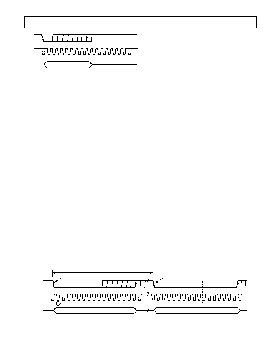
Figure 22. Entering Power-Down Mode
Once
CS has been brought high in this window of SCLKs, the
part will enter power-down, the conversion that was initiated by
the falling edge of
CS will be terminated, and SDATA will go
back into three-state. The time from the rising edge of
CS to
SDATA three-state enabled will never be greater than t8 (see
Timing Specifications). If
CS is brought high before the second
SCLK falling edge, the part will remain in normal mode and will
not power down. This will avoid accidental power-down due to
glitches on the
CS line.
To exit this mode of operation and power the AD7450 up again,
a dummy conversion is performed. On the falling edge of
CS, the
device will begin to power up and continue to power up as long
as
CS is held low until after the falling edge of the 10th SCLK. The
device will be fully powered up after 1
s has elapsed and, as
shown in Figure 23, valid data will result from the next conversion.
If
CS is brought high before the 10th falling edge of SCLK, the
AD7450 will again go back into power-down. This avoids
accidental power-up due to glitches on the
CS line or an
inadvertent burst of eight SCLK cycles while
CS is low. So although
the device may begin to power up on the falling edge of
CS, it will
again power down on the rising edge of
CS as long as it occurs
before the 10th SCLK falling edge.
Power-Up Time
The power-up time of the AD7450 is typically 1
s, which means
that with any frequency of SCLK up to 18 MHz, one dummy cycle
will always be sufficient to allow the device to power up. Once
the dummy cycle is complete, the ADC will be fully powered up
and the input signal will be acquired properly. The quiet time,
tQUIET, must still be allowed from the point at which the bus
goes back into three-state after the dummy conversion to the
next falling edge of
CS.
When running at the maximum throughput rate of 1 MSPS,
the AD7450 will power up and acquire a signal within
±0.5 LSB
in one dummy cycle, i.e., 1
s. When powering up from the
power-down mode with a dummy cycle, as in Figure 23, the
track-and-hold, which was in hold mode while the part was
powered down, returns to track mode after the first SCLK
edge the part receives after the falling edge of
CS. This is shown
as Point A in Figure 23.
Although at any SCLK frequency one dummy cycle is sufficient
to power the device up and acquire VIN, it does not necessarily
mean that a full dummy cycle of 16 SCLKs must always elapse
to power up the device and acquire VIN fully; 1
s will be
sufficient to power the device up and acquire the input signal.
For example, if a 5 MHz SCLK frequency was applied to the ADC,
the cycle time would be 3.2
s (i.e., 1/(5 MHz)
16). In one
dummy cycle, 3.2
s, the part would be powered up and VIN
acquired fully. However, after 1
s with a 5 MHz SCLK, only
5 SCLK cycles would have elapsed. At this stage, the ADC would
be fully powered up and the signal acquired. So, in this case, the
CS can be brought high after the 10th SCLK falling edge and
brought low again after a time, tQUIET, to initiate the conversion.
When power supplies are first applied to the AD7450, the ADC
may either power up in the power-down mode or normal mode.
Because of this, it is best to allow a dummy cycle to elapse to
ensure the part is fully powered up before attempting a valid
conversion. Likewise, if the user wishes the part to power up in
power-down mode, then the dummy cycle may be used to ensure
the device is in power-down by executing a cycle such as that
shown in Figure 22.
Once supplies are applied to the AD7450, the power-up time is
the same as that when powering up from the power-down mode.
It takes approximately 1
s to power up fully if the part powers
up in normal mode. It is not necessary to wait 1
s before
executing a dummy cycle to ensure the desired mode of operation.
Instead, the dummy cycle can occur directly after power is
supplied to the ADC. If the first valid conversion is then performed
directly after the dummy conversion, care must be taken to ensure
that adequate acquisition time has been allowed.
As mentioned earlier, when powering up from the power-down
mode, the part will return to track upon the first SCLK edge
applied after the falling edge of
CS. However, when the ADC
powers up initially after supplies are applied, the track-and-hold
will already be in track. This means if (assuming one has the
facility to monitor the ADC supply current) the ADC powers
up in the desired mode of operation, and thus a dummy cycle is
not required to change the mode, then a dummy cycle is not
required to place the track-and-hold into track.
SDATA
CS
INVALID DATA
SCLK
116
VALID DATA
1
A
THE PART BEGINS
TO POWER UP
THE PART IS FULLY POWERED
UP WITH V IN FULLY ACQUIRED
10
16
t
POWER-UP
Figure 23. Exiting Power-Down Mode
Rev. A
相关PDF资料 |
PDF描述 |
|---|---|
| VI-B5P-MW-S | CONVERTER MOD DC/DC 13.8V 100W |
| VI-B5M-MW-S | CONVERTER MOD DC/DC 10V 100W |
| VI-B52-MW-S | CONVERTER MOD DC/DC 15V 100W |
| AD7450ARMZ-REEL7 | IC ADC 12BIT DIFF IN 1MSPS 8MSOP |
| VI-2TL-MX-S | CONVERTER MOD DC/DC 28V 75W |
相关代理商/技术参数 |
参数描述 |
|---|---|
| AD7450BR | 制造商:Rochester Electronics LLC 功能描述:3V/5V DIFFERENTIAL INPUT 12 BIT SAR IC - Bulk |
| AD7450BRM | 制造商:Analog Devices 功能描述:ADC Single SAR 1Msps 12-bit Serial 8-Pin MSOP 制造商:Rochester Electronics LLC 功能描述:3V/5V DIFFERENTIAL INPUT 12 BIT SAR IC - Bulk 制造商:Analog Devices 功能描述:Analog-Digital Converter IC Number of Bi |
| AD7450BRM-REEL | 制造商:Analog Devices 功能描述:ADC Single SAR 1Msps 12-bit Serial 8-Pin MSOP T/R 制造商:Rochester Electronics LLC 功能描述:3V/5V DIFFERENTIAL INPUT 12 BIT SAR IC - Tape and Reel |
| AD7450BRM-REEL7 | 制造商:Analog Devices 功能描述:ADC Single SAR 1Msps 12-bit Serial 8-Pin MSOP T/R 制造商:Rochester Electronics LLC 功能描述:3V/5V DIFFERENTIAL INPUT 12 BIT SAR IC - Tape and Reel |
| AD7450BRMZ | 功能描述:IC ADC 12BIT DIFF IN 1MSPS 8MSOP RoHS:是 类别:集成电路 (IC) >> 数据采集 - 模数转换器 系列:- 标准包装:1,000 系列:- 位数:16 采样率(每秒):45k 数据接口:串行 转换器数目:2 功率耗散(最大):315mW 电压电源:模拟和数字 工作温度:0°C ~ 70°C 安装类型:表面贴装 封装/外壳:28-SOIC(0.295",7.50mm 宽) 供应商设备封装:28-SOIC W 包装:带卷 (TR) 输入数目和类型:2 个单端,单极 |
发布紧急采购,3分钟左右您将得到回复。