- 您现在的位置:买卖IC网 > PDF目录10314 > AD7450ARZ-REEL (Analog Devices Inc)IC ADC 12BIT DIFF IN 1MSPS 8SOIC PDF资料下载
参数资料
| 型号: | AD7450ARZ-REEL |
| 厂商: | Analog Devices Inc |
| 文件页数: | 7/22页 |
| 文件大小: | 0K |
| 描述: | IC ADC 12BIT DIFF IN 1MSPS 8SOIC |
| 标准包装: | 2,500 |
| 位数: | 12 |
| 采样率(每秒): | 1M |
| 数据接口: | DSP,MICROWIRE?,QSPI?,串行,SPI? |
| 转换器数目: | 1 |
| 功率耗散(最大): | 9.25mW |
| 电压电源: | 单电源 |
| 工作温度: | -40°C ~ 85°C |
| 安装类型: | 表面贴装 |
| 封装/外壳: | 8-SOIC(0.154",3.90mm 宽) |
| 供应商设备封装: | 8-SOIC |
| 包装: | 带卷 (TR) |
| 输入数目和类型: | 1 个差分,单极 |
| 配用: | EVAL-AD7450CBZ-ND - BOARD EVALUATION FOR AD7450 |
AD7450
–15–
SINGLE-ENDED OPERATION
When supplied with a 5 V power supply, the AD7450 can handle
a single-ended input. The design of this part is optimized for
differential operation, so with a single-ended input, performance
will degrade. Linearity will typically degrade by 0.2 LSBs, zero
code and full-scale errors will typically degrade by 2 LSBs, and
ac performance is not guaranteed.
To operate the AD7450 in single-ended mode, the VIN+ input is
coupled to the signal source, while the VIN– input is biased to the
appropriate voltage corresponding to the midscale code transi-
tion. This voltage is the common mode, which is a fixed dc
voltage (usually the reference). The VIN+ input swings around
this value and should have voltage span of 2
VREF to make use
of the full dynamic range of the part. Therefore, the input signal
will have peak-to-peak values of common mode
± V
REF. If the
analog input is unipolar then an op amp in a noninverting unity
gain configuration can be used to drive the VIN+ pin. Because
the ADC operates from a single supply, it is necessary to level
shift ground based bipolar signals to comply with the input
requirements. An op amp can be configured to rescale and level
shift the ground based bipolar signal so it is compatible with the
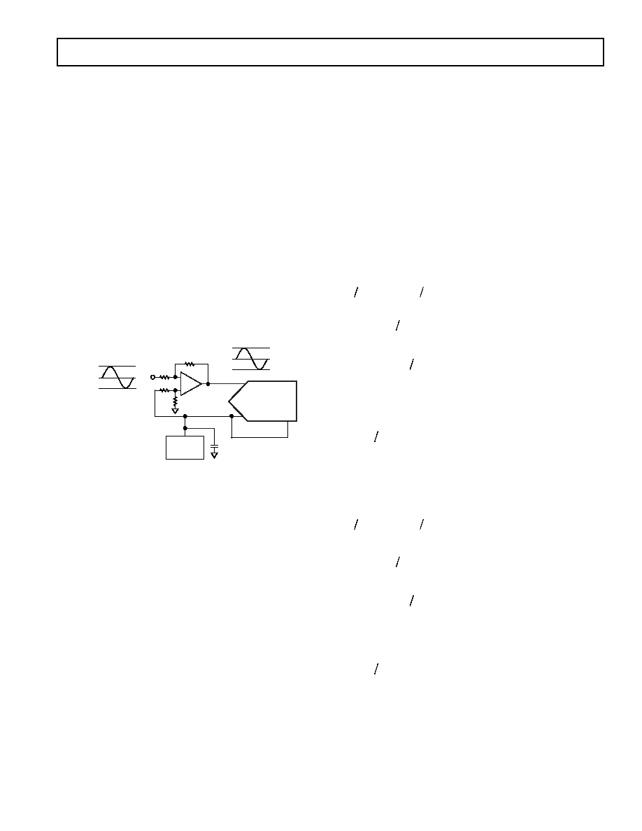
selected input range of the AD7450 (see Figure 18).
+
–
R
0.1 F
VIN
EXTERNAL
VREF (2.5V)
AD7450
VIN+
VIN–
VREF
+2.5V
–2.5V
0V
5V
0V
2.5V
Figure 18. Applying a Bipolar Single-Ended
Input to the AD7450
SERIAL INTERFACE
Figure 19 shows a detailed timing diagram for the serial interface
of the AD7450. The serial clock provides the conversion clock
and also controls the transfer of data from the AD7450 during
conversion.
CS initiates the conversion process and frames the
data transfer. The falling edge of
CS puts the track-and-hold into
hold mode and takes the bus out of three-state. The analog input
is sampled and the conversion initiated at this point. The
conversion will require 16 SCLK cycles to complete.
Once 13 SCLK falling edges have occurred, the track-and-hold
will go back into track on the next SCLK rising edge as shown
at Point B in Figure 19. On the 16th SCLK falling edge, the
SDATA line will go back into three-state.
If the rising edge of
CS occurs before 16 SCLKs have elapsed,
the conversion will be terminated, and the SDATA line will go
back into three-state. Sixteen serial clock cycles are required to
perform a conversion and to access data from the AD7450.
CS
going low provides the first leading zero to be read in by the
microcontroller or DSP. The remaining data is then clocked out
on the subsequent SCLK falling edges beginning with the second
leading zero. Thus, the first falling clock edge on the serial clock
provides the second leading zero. The final bit in the data transfer
is valid on the 16th falling edge, having been clocked out on the
previous (15th) falling edge. Once the conversion is complete
and the data has been accessed after the 16 clock cycles, it is
important to ensure that before the next conversion is initiated,
enough time is left to meet the acquisition and quiet time speci-
fications (see timing examples). To achieve 1 MSPS with an 18
MHz clock for VDD = 5 V, an 18 clock burst will perform the
conversion and leave enough time before the next conversion for
the acquisition and quiet time. This is the same for achieving
833 kSPS with a 15 MHz clock for VDD = 3 V.
In applications with a slower SCLK, it may be possible to read
in data on each SCLK rising edge, i.e., the first rising edge of
SCLK after the
CS falling edge would have the leading zero
provided and the 15th SCLK edge would have DB0 provided.
Timing Example 1
Having fSCLK = 18 MHz and a throughput rate of 1 MSPS gives
a cycle time of:
11 1 000 000
1
Throughput
s
==
,,
A cycle consists of:
tf
t
SCLK
ACQ
2
12 5 1
1
+
() +=
.
s
Therefore, if t2 = 10 ns then:
10
12 5 1 18
1
ns
MHz
t
s
ACQ
+
() +=
.
tns
ACQ
= 296
This 296 ns satisfies the requirement of 200 ns for tACQ. From
Figure 20, tACQ is comprised of:
2
8
.51 f
SCLK
() ++
tt
QUIET
where t8 = 35 ns. This allows a value of 122 ns for tQUIET, satis-
fying the minimum requirement of 25 ns.
Timing Example 2
Having fSCLK = 5 MHz and a throughput rate of 315 kSPS gives
a cycle time of:
11 315 000
3 174
Throughput
s
==
,.
A cycle consists of:
tf
t
SCLK
ACQ
2
12 5 1
3 174
+
() +=
..
s
Therefore if t2 is 10 ns then:
10
12 5 1 5
3 174
ns
MHz
t
s
ACQ
+
() +=
..
tns
ACQ
= 664
This 664 ns satisfies the requirement of 200 ns for tACQ. From
Figure 20, tACQ is comprised of:
2
8
.51 f
SCLK
() ++
tt
QUIET
where t8 = 35 ns. This allows a value of 129 ns for tQUIET, satis-
fying the minimum requirement of 25 ns.
As in this example and with other slower clock values, the signal
may already be acquired before the conversion is complete, but it
is still necessary to leave 25 ns minimum tQUIET between conver-
sions. In Timing Example 2, the signal should be fully acquired
at approximately Point C in Figure 20.
Rev. A
相关PDF资料 |
PDF描述 |
|---|---|
| VE-B3X-MY | CONVERTER MOD DC/DC 5.2V 50W |
| VE-B3W-MY | CONVERTER MOD DC/DC 5.5V 50W |
| VE-B3T-MY | CONVERTER MOD DC/DC 6.5V 50W |
| VE-B3R-MY | CONVERTER MOD DC/DC 7.5V 50W |
| VE-B30-MY | CONVERTER MOD DC/DC 5V 50W |
相关代理商/技术参数 |
参数描述 |
|---|---|
| AD7450ARZ-REEL7 | 功能描述:IC ADC 12BIT DIFF IN 1MSPS 8SOIC RoHS:是 类别:集成电路 (IC) >> 数据采集 - 模数转换器 系列:- 标准包装:1,000 系列:- 位数:16 采样率(每秒):45k 数据接口:串行 转换器数目:2 功率耗散(最大):315mW 电压电源:模拟和数字 工作温度:0°C ~ 70°C 安装类型:表面贴装 封装/外壳:28-SOIC(0.295",7.50mm 宽) 供应商设备封装:28-SOIC W 包装:带卷 (TR) 输入数目和类型:2 个单端,单极 |
| AD7450BR | 制造商:Rochester Electronics LLC 功能描述:3V/5V DIFFERENTIAL INPUT 12 BIT SAR IC - Bulk |
| AD7450BRM | 制造商:Analog Devices 功能描述:ADC Single SAR 1Msps 12-bit Serial 8-Pin MSOP 制造商:Rochester Electronics LLC 功能描述:3V/5V DIFFERENTIAL INPUT 12 BIT SAR IC - Bulk 制造商:Analog Devices 功能描述:Analog-Digital Converter IC Number of Bi |
| AD7450BRM-REEL | 制造商:Analog Devices 功能描述:ADC Single SAR 1Msps 12-bit Serial 8-Pin MSOP T/R 制造商:Rochester Electronics LLC 功能描述:3V/5V DIFFERENTIAL INPUT 12 BIT SAR IC - Tape and Reel |
| AD7450BRM-REEL7 | 制造商:Analog Devices 功能描述:ADC Single SAR 1Msps 12-bit Serial 8-Pin MSOP T/R 制造商:Rochester Electronics LLC 功能描述:3V/5V DIFFERENTIAL INPUT 12 BIT SAR IC - Tape and Reel |
发布紧急采购,3分钟左右您将得到回复。