- 您现在的位置:买卖IC网 > PDF目录10672 > AD7476AYKSZ-500RL7 (Analog Devices Inc)IC ADC 12BIT 1MSPS SC70-6 PDF资料下载
参数资料
| 型号: | AD7476AYKSZ-500RL7 |
| 厂商: | Analog Devices Inc |
| 文件页数: | 8/29页 |
| 文件大小: | 0K |
| 描述: | IC ADC 12BIT 1MSPS SC70-6 |
| 设计资源: | Output Channel Monitoring Using AD5380 (CN0008) AD5382 Channel Monitor Function (CN0012) AD5381 Channel Monitor Function (CN0013) AD5383 Channel Monitor Function (CN0015) AD5390/91/92 Channel Monitor Function (CN0030) Power off protected data acquisition signal chain using ADG4612 , AD711, and AD7476 (CN0165) |
| 标准包装: | 1 |
| 位数: | 12 |
| 采样率(每秒): | 1M |
| 数据接口: | DSP,MICROWIRE?,QSPI?,串行,SPI? |
| 转换器数目: | 1 |
| 功率耗散(最大): | 17.5mW |
| 电压电源: | 单电源 |
| 工作温度: | -40°C ~ 85°C |
| 安装类型: | 表面贴装 |
| 封装/外壳: | 6-TSSOP,SC-88,SOT-363 |
| 供应商设备封装: | SC-70-6 |
| 包装: | 标准包装 |
| 输入数目和类型: | 1 个单端,单极 |
| 其它名称: | AD7476AYKSZ-500RL7DKR AD7476AYKSZ500RL7DKR AD7476AYKSZ500RL7DKR-ND |
第1页第2页第3页第4页第5页第6页第7页当前第8页第9页第10页第11页第12页第13页第14页第15页第16页第17页第18页第19页第20页第21页第22页第23页第24页第25页第26页第27页第28页第29页
AD7476A/AD7477A/AD7478A
Rev. F | Page 15 of 28
THEORY OF OPERATION
CIRCUIT INFORMATION
The AD7476A/AD7477A/AD7478A are fast, micropower,
12-/10-/8-bit, single-supply analog-to-digital converters (ADCs),
respectively. The parts can be operated from a 2.35 V to 5.25 V
supply. When operated from either a 5 V supply or a 3 V supply,
the AD7476A/AD7477A/AD7478A are capable of throughput
rates of 1 MSPS when provided with a 20 MHz clock. The
AD7476A/AD7477A/AD7478A provide the user with an on-
chip, track-and-hold ADC and a serial interface housed in a
tiny 6-lead SC70 or 8-lead MSOP package, offering the user
considerable space-saving advantages over alternative solutions.
The serial clock input accesses data from the part but also pro-
vides the clock source for the successive-approximation ADC.
The analog input range is 0 V to VDD. The ADC does not require
an external reference or an on-chip reference. The reference for
the AD7476A/AD7477A/AD7478A is derived from the power
supply and, thus, gives the widest dynamic input range. The
AD7476A/AD7477A/AD7478A also feature a power-down
option to allow power saving between conversions. The power-
down feature is implemented across the standard serial interface,
as described in the Modes of Operation section.
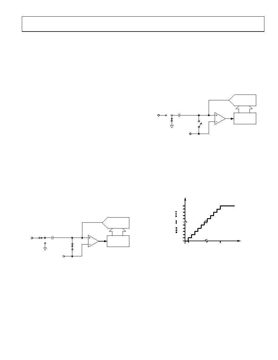
THE CONVERTER OPERATION
AD7476A/AD7477A/AD7478A are successive approximation,
analog-to-digital converters based around a charge redistribu-
tion DAC. Figure 15 and Figure 16 show simplified schematics
of the ADC. Figure 15 shows the ADC during its acquisition
phase. SW2 is closed and SW1 is in Position A, the comparator
is held in a balanced condition, and the sampling capacitor
acquires the signal on VIN.
CHARGE
REDISTRIBUTION
DAC
CONTROL
LOGIC
COMPARATOR
SW2
SAMPLING
CAPACITOR
ACQUISITION
PHASE
SW1
A
B
AGND
VDD/2
VIN
02930-015
Figure 15. ADC Acquisition Phase
When the ADC starts a conversion (see Figure 16), SW2 opens
and SW1 moves to Position B, causing the comparator to become
unbalanced. The control logic and the charge redistribution
DAC are used to add and subtract fixed amounts of charge from
the sampling capacitor to bring the comparator back into a
balanced condition. When the comparator is rebalanced, the
conversion is complete. The control logic generates the ADC
output code. Figure 17 shows the ADC transfer function.
CHARGE
REDISTRIBUTION
DAC
CONTROL
LOGIC
COMPARATOR
SW2
SAMPLING
CAPACITOR
CONVERSION
PHASE
SW1
A
B
AGND
VDD/2
VIN
02930-016
Figure 16. ADC Conversion Phase
ADC TRANSFER FUNCTION
The output coding of the AD7476A/AD7477A/AD7478A is
straight binary. The designed code transitions occur at the
successive integer LSB values, that is, 1 LSB, 2 LSB, and so on.
The LSB size is VDD/4096 for the AD7476A, VDD/1024 for the
AD7477A, and VDD/256 for the AD7478A. The ideal transfer
characteristic for the AD7476A/AD7477A/AD7478A is shown
000...000
0V
ADC
CODE
ANALOG INPUT
111...111
000...001
000...010
111...110
111...000
011...111
1LSB = VDD/256 (AD7478A)
1LSB
+VDD – 1LSB
1LSB = VDD/1024 (AD7477A)
1LSB = VDD/4096 (AD7476A)
02930-017
Figure 17. AD7476A/AD7477A/AD7478A
Transfer Characteristic
相关PDF资料 |
PDF描述 |
|---|---|
| NCS2200SN2T1G | IC COMPARATOR 1V LOW PWR 5TSOP |
| DS90CR218AMTD/NOPB | IC RCVR 21BIT CHAN LINK 48TSSOP |
| LTC2440IGN#PBF | IC ADC DIFFER 24-BIT HS 16-SSOP |
| VE-B1T-MX-F1 | CONVERTER MOD DC/DC 6.5V 75W |
| VE-J5K-MY-F4 | CONVERTER MOD DC/DC 40V 50W |
相关代理商/技术参数 |
参数描述 |
|---|---|
| AD7476AYKSZ-500RL73 | 制造商:AD 制造商全称:Analog Devices 功能描述:2.35 V to 5.25 V, 1 MSPS, 12-/10-/8-Bit ADCs in 6-Lead SC70 |
| AD7476AYKSZ-REEL7 | 功能描述:IC ADC 12BIT 1MSPS SC70-6 RoHS:是 类别:集成电路 (IC) >> 数据采集 - 模数转换器 系列:- 标准包装:1,000 系列:- 位数:16 采样率(每秒):45k 数据接口:串行 转换器数目:2 功率耗散(最大):315mW 电压电源:模拟和数字 工作温度:0°C ~ 70°C 安装类型:表面贴装 封装/外壳:28-SOIC(0.295",7.50mm 宽) 供应商设备封装:28-SOIC W 包装:带卷 (TR) 输入数目和类型:2 个单端,单极 |
| AD7476AYKSZ-REEL73 | 制造商:AD 制造商全称:Analog Devices 功能描述:2.35 V to 5.25 V, 1 MSPS, 12-/10-/8-Bit ADCs in 6-Lead SC70 |
| AD7476AYRM | 制造商:Analog Devices 功能描述:ADC Single SAR 1Msps 12-bit Serial 8-Pin MSOP 制造商:Rochester Electronics LLC 功能描述:12-BIT LOW VOLTAGE, LOW POWER ADC I.C. - Bulk |
| AD7476AYRM-REEL7 | 制造商:Analog Devices 功能描述:ADC Single SAR 1Msps 12-bit Serial 8-Pin MSOP T/R 制造商:Rochester Electronics LLC 功能描述:12-BIT LOW VOLTAGE, LOW POWER ADC I.C. - Tape and Reel |
发布紧急采购,3分钟左右您将得到回复。