- 您现在的位置:买卖IC网 > PDF目录373901 > AD7478AAKSZ-REEL (ANALOG DEVICES INC) Circular Connector; MIL SPEC:MIL-C-5015; Body Material:Metal; Series:GT; No. of Contacts:3; Connector Shell Size:28; Connecting Termination:Solder; Circular Shell Style:Square Flange Receptacle; Body Style:Straight PDF资料下载
参数资料
| 型号: | AD7478AAKSZ-REEL |
| 厂商: | ANALOG DEVICES INC |
| 元件分类: | ADC |
| 英文描述: | Circular Connector; MIL SPEC:MIL-C-5015; Body Material:Metal; Series:GT; No. of Contacts:3; Connector Shell Size:28; Connecting Termination:Solder; Circular Shell Style:Square Flange Receptacle; Body Style:Straight |
| 中文描述: | 1-CH 8-BIT SUCCESSIVE APPROXIMATION ADC, SERIAL ACCESS, PDSO6 |
| 封装: | ROHS COMPLIANT, MO-203AB, SC-70, 6 PIN |
| 文件页数: | 16/24页 |
| 文件大小: | 580K |
| 代理商: | AD7478AAKSZ-REEL |
REV. C
–16–
AD7476A/AD7477A/AD7478A
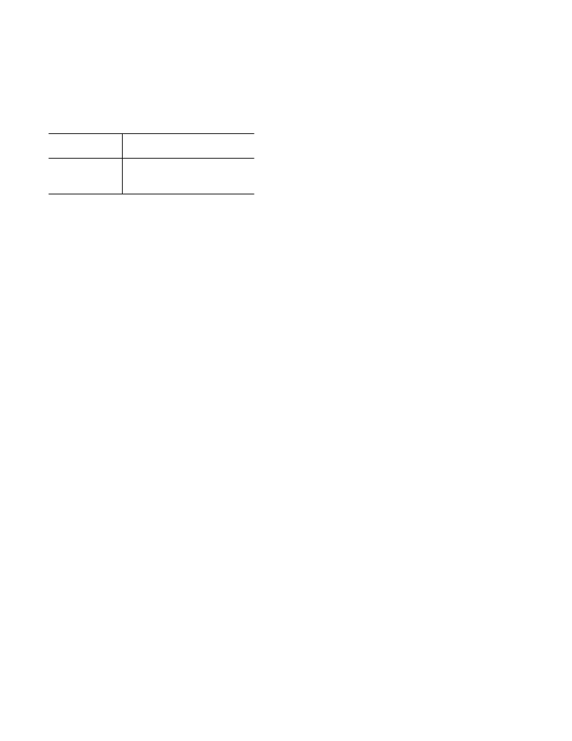
Table II provides some typical performance data with various
op amps used as the input buffer for a 100 kHz input tone at
room temperature under the same setup conditions.
Table II. AD7476A Typical Performance with Various
Input Buffers, V
DD
= 3 V
Op Amp in the
Input Buffer
AD7476A SNR Performance
(dB)
AD711
AD797
AD845
72.3
72.5
71.4
When no amplifier is used to drive the analog input, the source
impedance should be limited to low values. The maximum
source impedance will depend on the amount of total harmonic
distortion (THD) that can be tolerated. The THD will increase
as the source impedance increases and the performance will
degrade. See TPC 7.
Digital Inputs
The digital inputs applied to the AD7476A/AD7477A/AD7478A
are not limited by the maximum ratings that limit the analog
input. Instead, the digital inputs applied can go to 7 V and are
not restricted by the V
DD
+ 0.3 V limit as on the analog input.
For example, if the AD7476A/AD7477A/AD7478A were oper-
ated with a V
DD
of 3 V, then 5 V logic levels could be used on
the digital inputs. However, it is important to note that the data
output on SDATA will still have 3 V logic levels when V
DD
= 3 V.
Another advantage of SCLK and
CS
not being restricted by the
V
DD
+ 0.3 V limit is the fact that power supply sequencing
issues are avoided. If
CS
or SCLK is applied before V
DD
, there
is no risk of latch-up as there would be on the analog input if a
signal greater than 0.3 V was applied prior to V
DD
.
MODES OF OPERATION
The mode of operation of the AD7476A/AD7477A/AD7478A is
selected by controlling the (logic) state of the
CS
signal during a
conversion. There are two possible modes of operation: normal
and power-down. The point at which
CS
is pulled high after the
conversion has been initiated will determine whether the
AD7476A/AD7477A/AD7478A will enter power-down mode or
not. Similarly, if already in power-down,
CS
can control
whether the device will return to normal operation or remain in
power-down. These modes of operation are designed to provide
flexible power management options. These options can be
chosen to optimize the power dissipation/throughput rate ratio for
different application requirements.
Normal Mode
This mode is intended for the fastest throughput rate perfor-
mance; the user does not have to worry about any power-up
times with the AD7476A/AD7477A/AD7478A remaining fully
powered all the time. Figure 9 shows the general diagram of the
operation of the AD7476A/AD7477A/AD7478A in this mode.
The conversion is initiated on the falling edge of
CS
as described
in the Serial Interface section. To ensure that the part remains
fully powered up at all times,
CS
must remain low until at least
10 SCLK falling edges have elapsed after the falling edge of
CS
.
If
CS
is brought high any time after the 10th SCLK falling edge
but before the end of the t
CONVERT
, the part will remain pow-
ered up, but the conversion
will be terminated and SDATA will
go back into three-state.
For the AD7476A, 16 serial clock cycles are required to com-
plete the conversion and access the complete conversion results.
For the AD7477A and AD7478A, a minimum of 14 and 12
serial clock cycles are required to complete the conversion and
access the complete conversion results, respectively.
CS
may idle high until the next conversion or may idle low until
CS
returns high sometime prior to the next conversion (effec-
tively idling
CS
low).
Once a data transfer is complete (SDATA has returned to
three-state), another conversion can be initiated after the quiet
time, t
QUIET
, has elapsed by bringing
CS
low again.
Power-Down Mode
This mode is intended for use in applications where slower
throughput rates are required; either the ADC is powered down
between each conversion, or a series of conversions is performed
at a high throughput rate and the ADC is then powered down
for a relatively long duration between these bursts of several
conversions. When the AD7476A/AD7477A/AD7478A is in
power-down, all analog circuitry is powered down.
To enter power-down, the conversion process must be inter-
rupted by bringing
CS
high anywhere after the second falling
edge of SCLK and before the 10th falling edge of SCLK, as
shown in Figure 10. Once
CS
has been brought high in this
window of SCLKs, the part will enter power-down, the con-
version that was initiated by the falling edge of
CS
will be
terminated, and SDATA will go back into three-state. If
CS
is
brought high before the second SCLK falling edge, the part will
remain in normal mode and will not power down. This will
avoid accidental power-down due to glitches on the
CS
line.
In order to exit this mode of operation and power up the
AD7476A/AD7477A/AD7478A again, a dummy conversion is
performed. On the falling edge of
CS
, the device will begin to
power up and will continue to power up as long as
CS
is held low
until after the falling edge of the 10th SCLK. The device will be
fully powered up once 16 SCLKs have elapsed, and valid data
will result from the next conversion as shown in Figure 11. If
CS
is brought high before the 10th falling edge of SCLK, then the
AD7476A/AD7477A/AD7478A will go back into power-down.
This avoids accidental power-up due to glitches on the
CS
line or
an inadvertent burst of eight SCLK cycles while
CS
is low. So
although the device may begin to power up on the falling edge of
CS
, it will power down again on the rising edge of
CS
as long as it
occurs before the 10th SCLK falling edge.
Power-Up Time
The power-up time of the AD7476A/AD7477A/AD7478A is
1
μ
s, which means that with any frequency of SCLK up to 20 MHz,
one dummy cycle will always be sufficient to allow the device to
power up. Once the dummy cycle is complete, the ADC will be
fully powered up and the input signal will be acquired properly.
The quiet time, t
QUIET
, must still be allowed from the point
where the bus goes back into three-state after the dummy con-
version to the next falling edge of
CS
. When running at a 1 MSPS
throughput rate, the AD7476A/AD7477A/AD7478A will power
up and acquire a signal within
±
0.5 LSB in one dummy
cycle, i.e., 1
μ
s.
When powering up from the power-down mode with a dummy
cycle, as in Figure 11, the track-and-hold that was in hold mode
while the part was powered down returns to track mode after
the first SCLK edge the part receives after the falling edge of
CS
. This is shown as Point A in Figure 11. Although at any
相关PDF资料 |
PDF描述 |
|---|---|
| AD7477AAKSZ-REEL7 | GT 12C 6#12 6#16 PIN RECP WALL |
| AD7478AAKSZ-REEL7 | GT 12C 6#12 6#16 SKT RECP WALL |
| AD7476AYKSZ-REEL7 | 2.35 V to 5.25 V, 1 MSPS, 12-/10-/8-Bit ADCs in 6-Lead SC70 |
| AD7476SRTZ-R2 | PTSE 11C 11#16 STR PLUG |
| AD7476ART-500RL7 | 1 MSPS, 12-/10-/8-Bit ADCs in 6-Lead SOT-23 |
相关代理商/技术参数 |
参数描述 |
|---|---|
| AD7478AAKSZ-REEL3 | 制造商:AD 制造商全称:Analog Devices 功能描述:2.35 V to 5.25 V, 1 MSPS, 12-/10-/8-Bit ADCs in 6-Lead SC70 |
| AD7478AAKSZ-REEL7 | 功能描述:IC ADC 8BIT 1MSPS SC70-6 T/R RoHS:是 类别:集成电路 (IC) >> 数据采集 - 模数转换器 系列:- 标准包装:2,500 系列:- 位数:16 采样率(每秒):15 数据接口:MICROWIRE?,串行,SPI? 转换器数目:1 功率耗散(最大):480µW 电压电源:单电源 工作温度:-40°C ~ 85°C 安装类型:表面贴装 封装/外壳:38-WFQFN 裸露焊盘 供应商设备封装:38-QFN(5x7) 包装:带卷 (TR) 输入数目和类型:16 个单端,双极;8 个差分,双极 配用:DC1011A-C-ND - BOARD DELTA SIGMA ADC LTC2494 |
| AD7478AAKSZ-REEL73 | 制造商:AD 制造商全称:Analog Devices 功能描述:2.35 V to 5.25 V, 1 MSPS, 12-/10-/8-Bit ADCs in 6-Lead SC70 |
| AD7478AARM | 功能描述:IC ADC 8BIT 2.35V 1MSPS 8-MSOP RoHS:否 类别:集成电路 (IC) >> 数据采集 - 模数转换器 系列:- 标准包装:2,500 系列:- 位数:16 采样率(每秒):15 数据接口:MICROWIRE?,串行,SPI? 转换器数目:1 功率耗散(最大):480µW 电压电源:单电源 工作温度:-40°C ~ 85°C 安装类型:表面贴装 封装/外壳:38-WFQFN 裸露焊盘 供应商设备封装:38-QFN(5x7) 包装:带卷 (TR) 输入数目和类型:16 个单端,双极;8 个差分,双极 配用:DC1011A-C-ND - BOARD DELTA SIGMA ADC LTC2494 |
| AD7478AARM-REEL | 制造商:Analog Devices 功能描述:ADC Single SAR 1.2Msps 8-bit Serial 8-Pin MSOP T/R 制造商:Analog Devices 功能描述:ADC SGL SAR 1.2MSPS 8BIT SERL 8MSOP - Tape and Reel 制造商:Rochester Electronics LLC 功能描述:8-BIT LOW POWER ADC IN USOIC PKG I.C - Tape and Reel |
发布紧急采购,3分钟左右您将得到回复。