- 您现在的位置:买卖IC网 > PDF目录10548 > AD7478AARMZ (Analog Devices Inc)IC ADC 8BIT 1MSPS 8-MSOP PDF资料下载
参数资料
| 型号: | AD7478AARMZ |
| 厂商: | Analog Devices Inc |
| 文件页数: | 9/29页 |
| 文件大小: | 0K |
| 描述: | IC ADC 8BIT 1MSPS 8-MSOP |
| 标准包装: | 50 |
| 位数: | 8 |
| 采样率(每秒): | 1M |
| 数据接口: | DSP,MICROWIRE?,QSPI?,串行,SPI? |
| 转换器数目: | 1 |
| 功率耗散(最大): | 17.5mW |
| 电压电源: | 单电源 |
| 工作温度: | -40°C ~ 85°C |
| 安装类型: | 表面贴装 |
| 封装/外壳: | 8-TSSOP,8-MSOP(0.118",3.00mm 宽) |
| 供应商设备封装: | 8-MSOP |
| 包装: | 管件 |
| 输入数目和类型: | 1 个单端,单极 |
| 产品目录页面: | 778 (CN2011-ZH PDF) |
第1页第2页第3页第4页第5页第6页第7页第8页当前第9页第10页第11页第12页第13页第14页第15页第16页第17页第18页第19页第20页第21页第22页第23页第24页第25页第26页第27页第28页第29页
AD7476A/AD7477A/AD7478A
Rev. F | Page 16 of 28
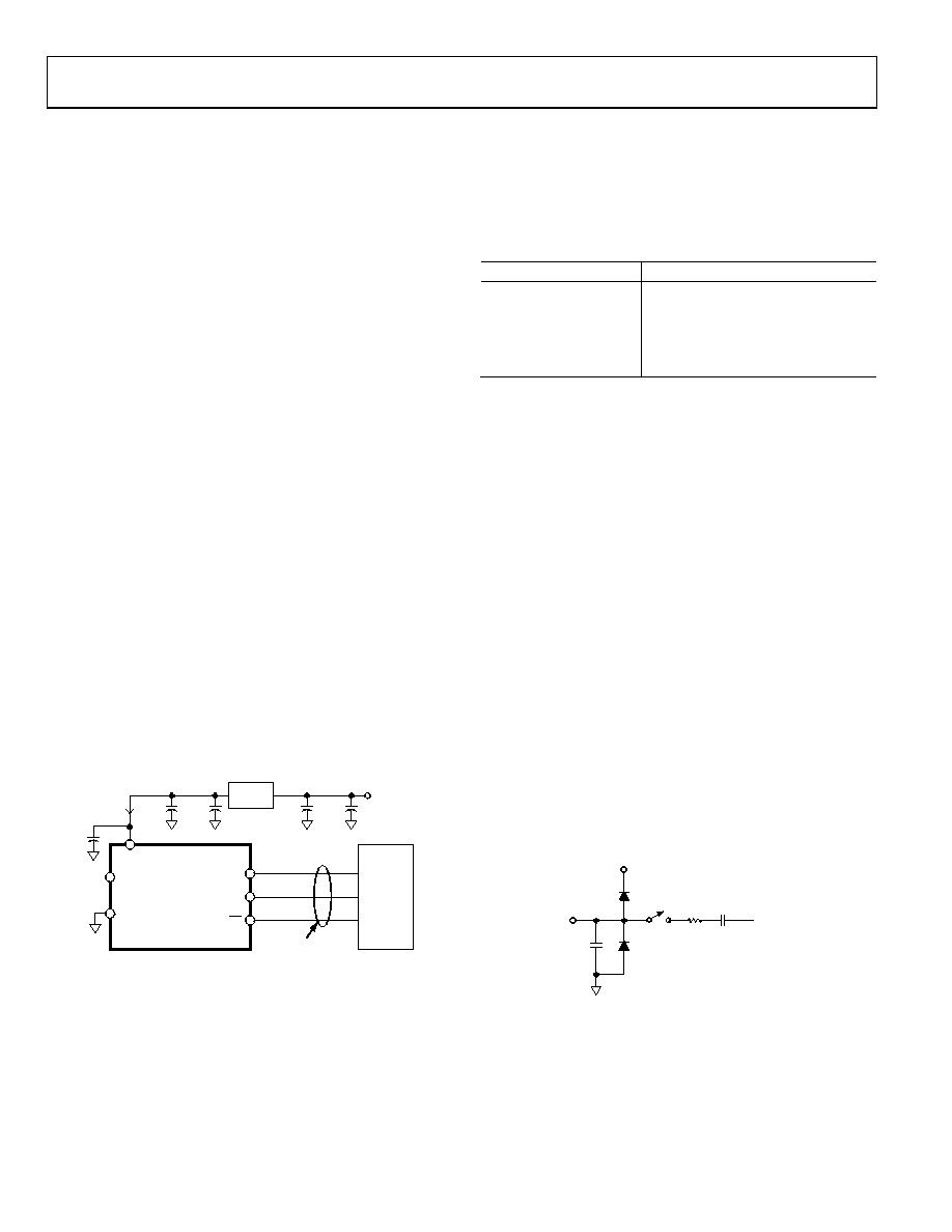
TYPICAL CONNECTION DIAGRAM
Figure 18 shows a typical connection diagram for the AD7476A/
AD7477A/AD7478A. VREF is taken internally from VDD and, as
such, VDD should be well decoupled. This provides an analog
input range of 0 V to VDD. The conversion result is output in a
16-bit word with four leading zeros followed by the MSB of the
12-bit, 10-bit, or 8-bit result. The 10-bit result from the AD7477A
is followed by two trailing zeros, and the 8-bit result from the
AD7478A is followed by four trailing zeros. Alternatively, because
the supply current required by the AD7476A/AD7477A/AD7478A
is so low, a precision reference can be used as the supply source
to the AD7476A/AD7477A/AD7478A. A REF19x voltage refer-
the required voltage to the ADC (see Figure 18). This configuration
is especially useful if the power supply is quite noisy, or if the
system supply voltages are at some value other than 5 V or 3 V
(for example, 15 V).
The REF19x outputs a steady voltage to the AD7476A/
AD7477A/AD7478A. If the low dropout REF193 is used, the
current it needs to supply to the AD7476A/AD7477A/ AD7478A is
typically 1.2 mA. When the ADC is converting at a rate of 1
MSPS, the REF193 needs to supply a maximum of 1.7 mA to the
AD7476A/AD7477A/AD7478A. The load regulation of the
of 17 ppm (51 V) for the 1.7 mA drawn from it. This corresponds
to a 0.069 LSB error for the AD7476A with VDD = 3 V from the
REF193, a 0.017 LSB error for the AD7477A, and a 0.0043 LSB
error for the AD7478A.
For applications where power consumption is a concern, use the
power-down mode of the ADC and the sleep mode of the
REF19x reference to improve power performance. See the
Modes of Operation section.
AD7476A/
AD7477A/
AD7478A
SCLK
SDATA
CS
VIN
GND
0V TO VDD
INPUT
VDD
C/P
SERIAL
INTERFACE
0.1
F
1
F
TANT
REF193
1.2mA
680nF
10
F
0.1
F
3V
5V
SUPPLY
02930-018
Figure 18. REF193 as Power Supply to AD7476A/
AD7477A/AD7478A
Table 7 provides typical performance data with various
references used as a VDD source for a 100 kHz input tone at
room temperature under the same setup conditions.
Table 7. AD7476A Typical Performance for Various Voltage
References
Reference Tied to VDD
AD7476A SNR Performance (dB)
AD780 @ 3 V
72.65
72.35
AD780 @ 2.5 V
72.5
72.2
72.6
ANALOG INPUT
Figure 19 shows an equivalent circuit of the analog input
structure of the AD7476A/AD7477A/AD7478A. The two
diodes, D1 and D2, provide ESD protection for the analog
input. Care must be taken to ensure that the analog input signal
never exceeds the supply rails by more than 300 mV. This
causes the diodes to become forward-biased and start
conducting current into the substrate. The maximum current
these diodes can conduct without causing irreversible damage
to the part is 10 mA. The Capacitor C1 in Figure 19 is typically
about 6 pF and can primarily be attributed to pin capacitance.
The Resistor R1 is a lumped component made up of the on
resistance of a switch. This resistor is typically about 100 . The
Capacitor C2 is the ADC sampling capacitor and has a
capacitance of 20 pF typically.
For ac applications, removing high frequency components from
the analog input signal is recommended by use of a band-pass
filter on the relevant analog input pin. In applications where
harmonic distortion and signal-to-noise ratio are critical, drive
the analog input from a low impedance source. Large source
impedances significantly affect the ac performance of the ADC,
necessitating the use of an input buffer amplifier. The choice of
the op amp is a function of the particular application.
D1
D2
R1
C2
20pF
VDD
VIN
C1
6pF
CONVERSION PHASE – SWITCH OPEN
TRACK PHASE – SWITCH CLOSED
02930-019
Figure 19. Equivalent Analog Input Circuit
相关PDF资料 |
PDF描述 |
|---|---|
| MS3102A16-7S | CONN RCPT 3POS BOX MNT W/SCKT |
| PT02SE-12-10P | CONN RECEPT 10POS W/PINS CRIMP |
| PT06E-14-19S | CONN PLUG 19 POS STRAIGHT W/SCKT |
| MS3102A22-6P | CONN RCPT 3POS BOX MNT W/PINS |
| PT02A-18-11P | CONN RCPT 11 POS BOX MNT W/PINS |
相关代理商/技术参数 |
参数描述 |
|---|---|
| AD7478AARMZ-REEL | 功能描述:IC ADC 8BIT 1MSPS 8-MSOP RoHS:是 类别:集成电路 (IC) >> 数据采集 - 模数转换器 系列:- 标准包装:2,500 系列:- 位数:16 采样率(每秒):15 数据接口:MICROWIRE?,串行,SPI? 转换器数目:1 功率耗散(最大):480µW 电压电源:单电源 工作温度:-40°C ~ 85°C 安装类型:表面贴装 封装/外壳:38-WFQFN 裸露焊盘 供应商设备封装:38-QFN(5x7) 包装:带卷 (TR) 输入数目和类型:16 个单端,双极;8 个差分,双极 配用:DC1011A-C-ND - BOARD DELTA SIGMA ADC LTC2494 |
| AD7478AARMZ-REEL7 | 功能描述:IC ADC 8BIT 1MSPS 8-MSOP RoHS:是 类别:集成电路 (IC) >> 数据采集 - 模数转换器 系列:- 标准包装:2,500 系列:- 位数:16 采样率(每秒):15 数据接口:MICROWIRE?,串行,SPI? 转换器数目:1 功率耗散(最大):480µW 电压电源:单电源 工作温度:-40°C ~ 85°C 安装类型:表面贴装 封装/外壳:38-WFQFN 裸露焊盘 供应商设备封装:38-QFN(5x7) 包装:带卷 (TR) 输入数目和类型:16 个单端,双极;8 个差分,双极 配用:DC1011A-C-ND - BOARD DELTA SIGMA ADC LTC2494 |
| AD7478ART | 制造商:Analog Devices 功能描述:ADC SGL SAR 1MSPS 8BIT SERL 6PIN SOT-23 - Bulk |
| AD7478ART-500RL7 | 功能描述:IC ADC 8BIT 1MSPS SOT-23-6 RoHS:否 类别:集成电路 (IC) >> 数据采集 - 模数转换器 系列:- 产品培训模块:Lead (SnPb) Finish for COTS Obsolescence Mitigation Program 标准包装:2,500 系列:- 位数:12 采样率(每秒):3M 数据接口:- 转换器数目:- 功率耗散(最大):- 电压电源:- 工作温度:- 安装类型:表面贴装 封装/外壳:SOT-23-6 供应商设备封装:SOT-23-6 包装:带卷 (TR) 输入数目和类型:- |
| AD7478ART-REEL | 制造商:AD 制造商全称:Analog Devices 功能描述:1 MSPS, 12-/10-/8-Bit ADCs in 6-Lead SOT-23 |
发布紧急采购,3分钟左右您将得到回复。