参数资料
| 型号: | AD7485BSTZ |
| 厂商: | Analog Devices Inc |
| 文件页数: | 15/15页 |
| 文件大小: | 0K |
| 描述: | IC ADC 14BIT SAR 1MSPS 48-LQFP |
| 标准包装: | 1 |
| 位数: | 14 |
| 采样率(每秒): | 1M |
| 数据接口: | 串行 |
| 转换器数目: | 1 |
| 功率耗散(最大): | 80mW |
| 电压电源: | 模拟和数字 |
| 工作温度: | -40°C ~ 85°C |
| 安装类型: | 表面贴装 |
| 封装/外壳: | 48-LQFP |
| 供应商设备封装: | 48-LQFP(7x7) |
| 包装: | 托盘 |
| 输入数目和类型: | 1 个单端,单极 |
REV.
–8–
AD7485
FREQUENCY – kHz
0
300
100
200
400
500
dB
–40
0
–60
–80
–20
–120
–100
–140
fIN = 10.7kHz
SNR = 78.76dB
SNR + D = 78.70dB
THD = –97.10dB
TPC 7. 64k FFT Plot with 10 kHz Input Tone
FREQUENCY – kHz
dB
–40
0
–60
–80
–20
–120
–100
–140
0
300
100
200
400
500
fIN = 507.3kHz
SNR = 78.35dB
SNR + D = 78.33dB
THD = –100.33dB
TPC 8. 64k FFT Plot with 500 kHz Input Tone
220
BIAS
VOLTAGE
1
2
3
4
5
6
7
8
AD8021
50
AC
SIGNAL
220
10pF
–VS
+VS
–
+
VIN
10pF
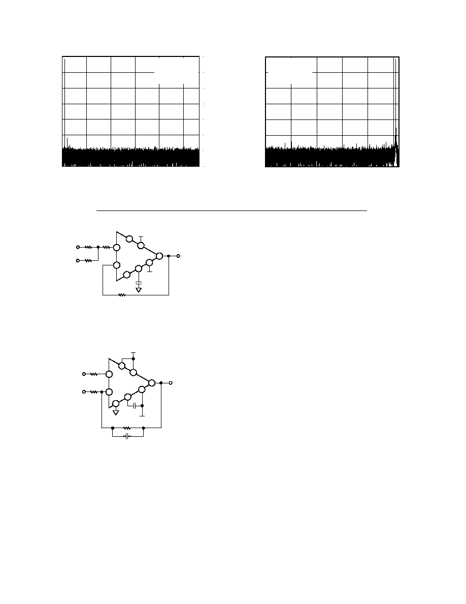
Figure 2. Analog Input Circuit Used for 500 kHz Input Tone
1
2
3
4
5
6
7
8
AD829
1k
100
AC
SIGNAL
BIAS
VOLTAGE
150
220pF
–VS
+VS
–
+
VIN
Figure 1. Analog Input Circuit Used for 10 kHz Input Tone
Figure 1 shows the analog input circuit used to obtain the data
for the FFT plot shown in TPC 7. The circuit uses an Analog
Devices AD829 op amp as the input buffer. A bipolar analog
signal is applied as shown and biased up with a stable, low noise
dc voltage connected to the labeled terminal shown. A 220 pF
compensation capacitor is connected between Pin 5 of the AD829
and the analog ground plane. The AD829 is supplied with +12 V
and –12 V supplies. The supply pins are decoupled as close to
the device as possible, with both a 0.1
F and 10 F capacitor
connected to each pin. In each case, the 0.1
F capacitor should be
the closer of the two capacitors to the device. More information
on the AD829 is available on the Analog Devices website.
For higher input bandwidth applications, Analog Devices’ AD8021
op amp (also available as a dual AD8022) is the recommended
choice to drive the AD7485. Figure 2 shows the analog input
circuit used to obtain the data for the FFT plot shown in TPC 8.
A bipolar analog signal is applied to the terminal shown and
biased with a stable, low noise dc voltage connected as shown. A
10 pF compensation capacitor is connected between Pin 5 of the
AD8021 and the negative supply. As with the previous circuit,
the AD8021 is supplied with +12 V and –12 V supplies. The
supply pins are decoupled as close to the device as possible with
both a 0.1
F and 10 F capacitor connected to each pin. In each
case, the 0.1
F capacitor should be the closer of the two capaci-
tors to the device. The AD8021 Logic Reference pin is tied to
analog ground and the
DISABLE pin is tied to the positive sup-
ply as shown. Detailed information on the AD8021 is available
on the Analog Devices website.
A
相关PDF资料 |
PDF描述 |
|---|---|
| AD7490BRU-REEL | IC ADC 12BIT 16CH 28-TSSOP T/R |
| AD7492ARZ-5 | IC ADC 12BIT REF/CLOCK 24SOIC |
| AD7495BRM | IC ADC 12BIT SRL LP W/REF 8MSOP |
| AD75004KP | IC DAC 12BIT QUAD W/BUFF 28-PLCC |
| AD7521LN | CONV D/A 12BIT 1MHZ 2LSB 18-DIP |
相关代理商/技术参数 |
参数描述 |
|---|---|
| AD7490 | 制造商:AD 制造商全称:Analog Devices 功能描述:16-Channel, 1 MSPS, 12-Bit ADC with Sequencer in 28-Lead TSSOP |
| AD7490_12 | 制造商:AD 制造商全称:Analog Devices 功能描述:16-Channel, 1 MSPS, 12-Bit ADC with Sequencer in 28-Lead TSSOP |
| AD7490BCP | 制造商:Analog Devices 功能描述:ADC Single SAR 1Msps 12-bit Serial 32-Pin LFCSP EP 制造商:Rochester Electronics LLC 功能描述:12 BIT 16 CHANNEL ADC IC - Bulk 制造商:Analog Devices 功能描述:IC 12-BIT ADC |
| AD7490BCP-REEL | 制造商:Analog Devices 功能描述:ADC Single SAR 1Msps 12-bit Serial 32-Pin LFCSP EP T/R |
| AD7490BCP-REEL7 | 制造商:Analog Devices 功能描述:ADC Single SAR 1Msps 12-bit Serial 32-Pin LFCSP EP T/R |
发布紧急采购,3分钟左右您将得到回复。