- 您现在的位置:买卖IC网 > PDF目录10673 > AD7490BCPZ (Analog Devices Inc)IC ADC 12BIT 16CH 32-LFCSP PDF资料下载
参数资料
| 型号: | AD7490BCPZ |
| 厂商: | Analog Devices Inc |
| 文件页数: | 13/29页 |
| 文件大小: | 0K |
| 描述: | IC ADC 12BIT 16CH 32-LFCSP |
| 产品变化通告: | IDD Specification Change 17/Jun/2009 |
| 标准包装: | 1 |
| 位数: | 12 |
| 采样率(每秒): | 1M |
| 数据接口: | DSP,MICROWIRE?,QSPI?,串行,SPI? |
| 转换器数目: | 1 |
| 功率耗散(最大): | 12.5mW |
| 电压电源: | 单电源 |
| 工作温度: | -40°C ~ 85°C |
| 安装类型: | 表面贴装 |
| 封装/外壳: | 32-VFQFN 裸露焊盘,CSP |
| 供应商设备封装: | 32-LFCSP-VQ |
| 包装: | 托盘 |
| 输入数目和类型: | 16 个单端,单极 |
| 产品目录页面: | 778 (CN2011-ZH PDF) |
第1页第2页第3页第4页第5页第6页第7页第8页第9页第10页第11页第12页当前第13页第14页第15页第16页第17页第18页第19页第20页第21页第22页第23页第24页第25页第26页第27页第28页第29页
Data Sheet
AD7490
Rev. D | Page 19 of 28
Reference Section
An external reference source should be used to supply the 2.5 V
reference to the AD7490. Errors in the reference source result
in gain errors in the AD7490 transfer function and add to the
specified full-scale errors of the part. A capacitor of at least 0.1 μF
should be placed on the REFIN pin. Suitable reference sources
for the AD7490 include the AD780, REF192, AD1582, ADR03,
ADR381, ADR391, and ADR421.
If 2.5 V is applied to the REFIN pin, the analog input range can
either be 0 V to 2.5 V or 0 V to 5 V, depending on the RANGE
bit in the control register.
MODES OF OPERATION
The AD7490 has a number of different modes of operation.
These modes are designed to provide flexible power manage-
ment options. These options can be chosen to optimize the
power dissipation/throughput rate ratio for differing application
requirements. The mode of operation of the AD7490 is controlled
by the power management bits, PM1 and PM0, in the control
register, as detailed in Table 7. When power supplies are first
applied to the AD7490, care should be taken to ensure that the
part is placed in the required mode of operation (see the
Powering Up the AD7490 section).
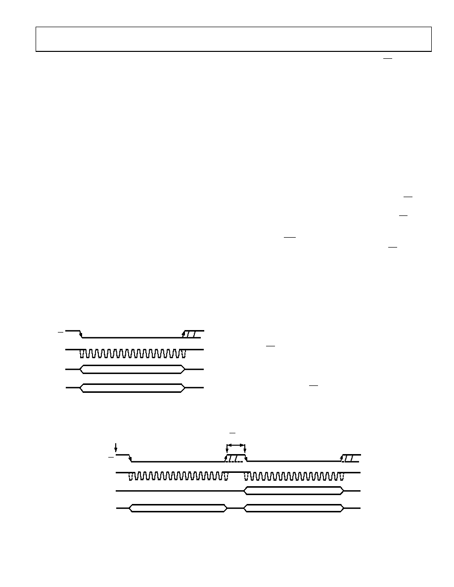
Normal Mode (PM1 = PM0 = 1)
This mode is intended for the fastest throughput rate performance
because the user does not have to worry about any power-up
times with the AD7490 remaining fully powered at all times.
Figure 22 shows the general diagram of the operation of the
AD7490 in this mode.
02
69
1-
0
21
NOTES
1. CONTROL REGISTER DATA IS LOADED ON FIRST 12 SCLK CYCLES
2. SHADOW REGISTER DATA IS LOADED ON FIRST 16 SCLK CYCLES
CS
SCLK
116
12
CHANNE L IDENTIFIER BITS + CONVERSION RESULT
DATA IN TO CONTROL/SHADOW REGISTER
DOUT
DIN
Figure 22. Normal Mode Operation
The conversion is initiated on the falling edge of CS, and the
track-and-hold enters hold mode, as described in the Serial
Interface section. The data presented to the AD7490 on the
DIN line during the first 12 clock cycles of the data transfer is
loaded
to the control register (provided the WRITE bit is 1). If data is
to be written to the Shadow register (SEQ = 0, SHADOW = 1
on previous write), data presented on the DIN line during the
first 16 SCLK cycles is loaded into the Shadow register. The part
remains fully powered up in normal mode at the end of the
conversion as long as PM1 and PM0 are set to 1 in the write
transfer during that conversion. To ensure continued operation
in normal mode, PM1 and PM0 are both loaded with 1 on every
data transfer. Sixteen serial clock cycles are required to complete
the conversion and access the conversion result. The track-and-
hold goes back into track on the 14th SCLK falling edge. CS may
then idle high until the next conversion or may idle low until
sometime prior to the next conversion, (effectively idling CS low).
Once a data transfer is complete (DOUT has returned to three-
state WEAK/TRI bit = 0), another conversion can be initiated
after the quiet time, tQUIET, has elapsed by bringing CS low again.
Full Shutdown (PM1 = 1, PM0 = 0)
In this mode, all internal circuitry on the AD7490 is powered
down. The part retains information in the control register
during full shutdown. The AD7490 remains in full shutdown
until the power management bits in the control register, PM1
and PM0, are changed.
If a write to the control register occurs while the part is in
full shutdown, with the power management bits changed to
PM0 = PM1 = 1 (normal mode), the part begins to power up
on the CS rising edge. The track-and-hold that was in hold
while the part was in full shutdown returns to track on the 14th
SCLK falling edge.
To ensure that the part is fully powered up, tPOWER UP (t12) should
elapse before the next CS falling edge. Figure 23 shows the
general diagram for this mode.
02
69
1-
B
-02
2
SCLK
116
1
14
16
14
DOUT
PART IS IN FULL
SHUTDOWN
PART BEGINS TO POWER UP ON CS
RISING EDGE AS PM1 = 1, PM0 = 1
PART IS FULLY POWERED UP
ONCE
tPOWER UP HAS ELAPSED
DIN
CS
t12
CHANNEL IDENTIFIER BITS + CONVERSION RESULT
DATA IN TO CONTROL REGISTER
CONTROL REGISTER IS LOADED ON THE
FIRST 12 CLOCKS, PM1 = 1, PM0 = 1
TO KEEP PART IN NORMAL MODE, LOAD
PM1 = 1, PM0 = 1 IN CONTROL REGISTER
DATA IN TO CONTROL/SHADOW REGISTER
Figure 23. Full Shutdown Mode Operation
相关PDF资料 |
PDF描述 |
|---|---|
| VE-J71-MY-F1 | CONVERTER MOD DC/DC 12V 50W |
| VE-B1V-MX-F1 | CONVERTER MOD DC/DC 5.8V 75W |
| VE-J70-MY-F4 | CONVERTER MOD DC/DC 5V 50W |
| VE-B1T-MX-F4 | CONVERTER MOD DC/DC 6.5V 75W |
| VE-J70-MY-F3 | CONVERTER MOD DC/DC 5V 50W |
相关代理商/技术参数 |
参数描述 |
|---|---|
| AD7490BCPZ | 制造商:Analog Devices 功能描述:IC, ADC, 12BIT, 1MSPS, LFCSP-32 |
| AD7490BCPZ-REEL7 | 功能描述:IC ADC 12BIT 16CHAN 32LFCSP RoHS:是 类别:集成电路 (IC) >> 数据采集 - 模数转换器 系列:- 标准包装:1,000 系列:- 位数:16 采样率(每秒):45k 数据接口:串行 转换器数目:2 功率耗散(最大):315mW 电压电源:模拟和数字 工作温度:0°C ~ 70°C 安装类型:表面贴装 封装/外壳:28-SOIC(0.295",7.50mm 宽) 供应商设备封装:28-SOIC W 包装:带卷 (TR) 输入数目和类型:2 个单端,单极 |
| AD7490BRU | 功能描述:IC ADC 12BIT 16CH 1MSPS 28TSSOP RoHS:否 类别:集成电路 (IC) >> 数据采集 - 模数转换器 系列:- 标准包装:1,000 系列:- 位数:12 采样率(每秒):300k 数据接口:并联 转换器数目:1 功率耗散(最大):75mW 电压电源:单电源 工作温度:0°C ~ 70°C 安装类型:表面贴装 封装/外壳:24-SOIC(0.295",7.50mm 宽) 供应商设备封装:24-SOIC 包装:带卷 (TR) 输入数目和类型:1 个单端,单极;1 个单端,双极 |
| AD7490BRU-REEL | 功能描述:IC ADC 12BIT 16CH 28-TSSOP T/R RoHS:否 类别:集成电路 (IC) >> 数据采集 - 模数转换器 系列:- 产品培训模块:Lead (SnPb) Finish for COTS Obsolescence Mitigation Program 标准包装:2,500 系列:- 位数:12 采样率(每秒):3M 数据接口:- 转换器数目:- 功率耗散(最大):- 电压电源:- 工作温度:- 安装类型:表面贴装 封装/外壳:SOT-23-6 供应商设备封装:SOT-23-6 包装:带卷 (TR) 输入数目和类型:- |
| AD7490BRU-REEL7 | 制造商:Analog Devices 功能描述:ADC Single SAR 1Msps 12-bit Serial 28-Pin TSSOP T/R 制造商:Analog Devices 功能描述:ADC SGL SAR 1MSPS 12-BIT SERL 28TSSOP - Tape and Reel 制造商:Rochester Electronics LLC 功能描述:12 BIT 16 CHANNEL ADC IC - Tape and Reel |
发布紧急采购,3分钟左右您将得到回复。