- 您现在的位置:买卖IC网 > PDF目录10673 > AD7490BCPZ (Analog Devices Inc)IC ADC 12BIT 16CH 32-LFCSP PDF资料下载
参数资料
| 型号: | AD7490BCPZ |
| 厂商: | Analog Devices Inc |
| 文件页数: | 15/29页 |
| 文件大小: | 0K |
| 描述: | IC ADC 12BIT 16CH 32-LFCSP |
| 产品变化通告: | IDD Specification Change 17/Jun/2009 |
| 标准包装: | 1 |
| 位数: | 12 |
| 采样率(每秒): | 1M |
| 数据接口: | DSP,MICROWIRE?,QSPI?,串行,SPI? |
| 转换器数目: | 1 |
| 功率耗散(最大): | 12.5mW |
| 电压电源: | 单电源 |
| 工作温度: | -40°C ~ 85°C |
| 安装类型: | 表面贴装 |
| 封装/外壳: | 32-VFQFN 裸露焊盘,CSP |
| 供应商设备封装: | 32-LFCSP-VQ |
| 包装: | 托盘 |
| 输入数目和类型: | 16 个单端,单极 |
| 产品目录页面: | 778 (CN2011-ZH PDF) |
第1页第2页第3页第4页第5页第6页第7页第8页第9页第10页第11页第12页第13页第14页当前第15页第16页第17页第18页第19页第20页第21页第22页第23页第24页第25页第26页第27页第28页第29页
Data Sheet
AD7490
Rev. D | Page 21 of 28
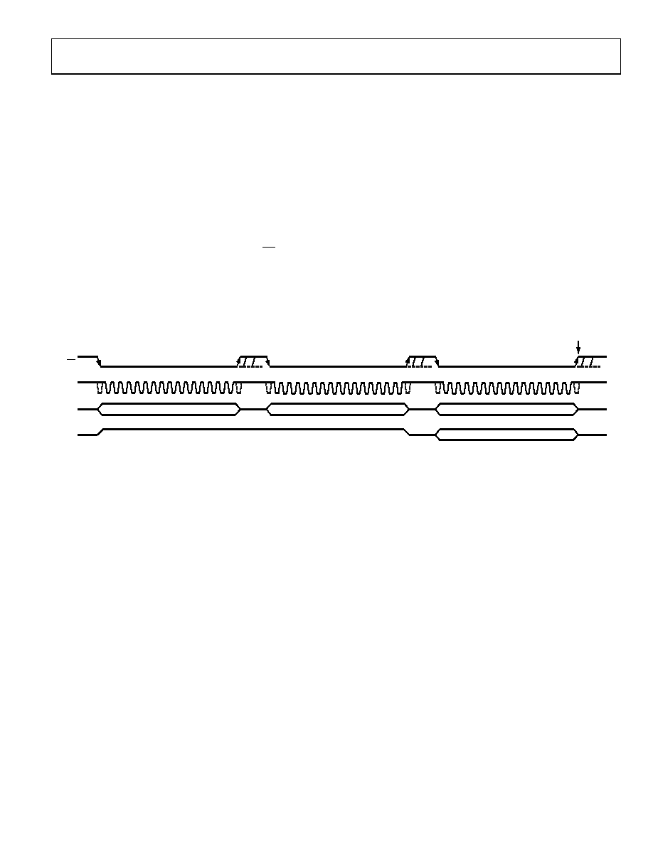
Powering Up the AD7490
When supplies are first applied to the AD7490, the ADC may
power up in any of the operating modes of the part. To ensure
that the part is placed into the required operating mode, the
user should perform a dummy cycle operation, as outlined in
The three dummy conversion operations outlined in Figure 26
must be performed to place the part into either of the auto modes.
The first two conversions of this dummy cycle operation are
performed with the DIN line tied high, and for the third conver-
sion of the dummy cycle operation, the user should write the
desired control register configuration to the AD7490 to place
the part into the required auto mode. On the third CS rising
edge after the supplies are applied, the control register contains
the correct information and valid data results from the next
conversion.
Therefore, to ensure the part is placed into the correct operating
mode when supplies are first applied to the AD7490, the user
must first issue two serial write operations with the DIN line
tied high. On the third conversion cycle, the user can then write
to the control register to place the part into any of the operating
modes. The user should not write to the Shadow register until
the fourth conversion cycle after the supplies are applied to
the ADC to guarantee that the control register contains the
correct data.
If the user wishes to place the part into either normal mode or
full shutdown mode, the second dummy cycle with DIN tied
high can be omitted from the three dummy conversion
operation outlined in Figure 26.
02
691
-02
5
SCLK
1
12
16
1
12
16
1
12
16
DOUT
DIN
CS
DUMMY CONVERSION
CORRECT VALUE IN CONTROL
REGISTER VALID DATA FROM
NEXT CONVERSION USER CAN
WRITE TO SHADOW REGISTER
IN NEXT CONVERSION
INVALID DATA
DATA IN TO CONTROL
CONTROL REGISTER IS LOADED ON THE
FIRST 12 CLOCK EDGES
KEEP DIN LINE TIED HIGH FOR FIRST TWO DUMMY CONVERSIONS
Figure 26. Placing into the Required Operating Mode After Supplies Are Applied
相关PDF资料 |
PDF描述 |
|---|---|
| VE-J71-MY-F1 | CONVERTER MOD DC/DC 12V 50W |
| VE-B1V-MX-F1 | CONVERTER MOD DC/DC 5.8V 75W |
| VE-J70-MY-F4 | CONVERTER MOD DC/DC 5V 50W |
| VE-B1T-MX-F4 | CONVERTER MOD DC/DC 6.5V 75W |
| VE-J70-MY-F3 | CONVERTER MOD DC/DC 5V 50W |
相关代理商/技术参数 |
参数描述 |
|---|---|
| AD7490BCPZ | 制造商:Analog Devices 功能描述:IC, ADC, 12BIT, 1MSPS, LFCSP-32 |
| AD7490BCPZ-REEL7 | 功能描述:IC ADC 12BIT 16CHAN 32LFCSP RoHS:是 类别:集成电路 (IC) >> 数据采集 - 模数转换器 系列:- 标准包装:1,000 系列:- 位数:16 采样率(每秒):45k 数据接口:串行 转换器数目:2 功率耗散(最大):315mW 电压电源:模拟和数字 工作温度:0°C ~ 70°C 安装类型:表面贴装 封装/外壳:28-SOIC(0.295",7.50mm 宽) 供应商设备封装:28-SOIC W 包装:带卷 (TR) 输入数目和类型:2 个单端,单极 |
| AD7490BRU | 功能描述:IC ADC 12BIT 16CH 1MSPS 28TSSOP RoHS:否 类别:集成电路 (IC) >> 数据采集 - 模数转换器 系列:- 标准包装:1,000 系列:- 位数:12 采样率(每秒):300k 数据接口:并联 转换器数目:1 功率耗散(最大):75mW 电压电源:单电源 工作温度:0°C ~ 70°C 安装类型:表面贴装 封装/外壳:24-SOIC(0.295",7.50mm 宽) 供应商设备封装:24-SOIC 包装:带卷 (TR) 输入数目和类型:1 个单端,单极;1 个单端,双极 |
| AD7490BRU-REEL | 功能描述:IC ADC 12BIT 16CH 28-TSSOP T/R RoHS:否 类别:集成电路 (IC) >> 数据采集 - 模数转换器 系列:- 产品培训模块:Lead (SnPb) Finish for COTS Obsolescence Mitigation Program 标准包装:2,500 系列:- 位数:12 采样率(每秒):3M 数据接口:- 转换器数目:- 功率耗散(最大):- 电压电源:- 工作温度:- 安装类型:表面贴装 封装/外壳:SOT-23-6 供应商设备封装:SOT-23-6 包装:带卷 (TR) 输入数目和类型:- |
| AD7490BRU-REEL7 | 制造商:Analog Devices 功能描述:ADC Single SAR 1Msps 12-bit Serial 28-Pin TSSOP T/R 制造商:Analog Devices 功能描述:ADC SGL SAR 1MSPS 12-BIT SERL 28TSSOP - Tape and Reel 制造商:Rochester Electronics LLC 功能描述:12 BIT 16 CHANNEL ADC IC - Tape and Reel |
发布紧急采购,3分钟左右您将得到回复。