参数资料
| 型号: | AD7537KRZ |
| 厂商: | Analog Devices Inc |
| 文件页数: | 4/10页 |
| 文件大小: | 0K |
| 描述: | IC DAC 12BIT DUAL MULT 24SOIC |
| 产品培训模块: | Data Converter Fundamentals DAC Architectures |
| 标准包装: | 31 |
| 设置时间: | 250µs |
| 位数: | 12 |
| 数据接口: | 并联 |
| 转换器数目: | 2 |
| 电压电源: | 单电源 |
| 功率耗散(最大): | 24mW |
| 工作温度: | -40°C ~ 85°C |
| 安装类型: | 表面贴装 |
| 封装/外壳: | 24-SOIC(0.295",7.50mm 宽) |
| 供应商设备封装: | 24-SOIC W |
| 包装: | 管件 |
| 输出数目和类型: | 2 电流,单极;2 电流,双极 |
| 采样率(每秒): | 667k |
AD7537
REV.
–3–
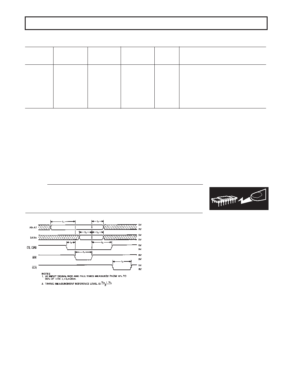
TIMING CHARACTERISTICS
Limit at
TA = –40 CTA = +55 C
Parameter
TA = +25 C
to +85 C
to +125 C
Units
Test Conditions/Comments
t1
15
30
ns min
Address Valid to Write Setup Time
t2
15
25
ns min
Address Valid to Write Hold Time
t3
60
80
ns min
Data Setup Time
t4
25
ns min
Data Hold Time
t5
0
ns min
Chip Select or Update to Write Setup Time
t6
0
ns min
Chip Select or Update to Write Hold Time
t7
80
100
ns min
Write Pulse Width
t8
80
100
ns min
Clear Pulse Width
Specifications subject to change without notice.
ABSOLUTE MAXIMUM RATINGS*
(TA = +25
°C unless otherwise stated)
VDD to DGND . . . . . . . . . . . . . . . . . . . . . . . . . . –0.3 V, +17 V
VREFA, VREFB to AGNDA, AGNDB . . . . . . . . . . . . . . . .
±25 V
VRFBA, VRFBB to AGNDA, AGNDB . . . . . . . . . . . . . . . .
±25 V
Digital Input Voltage to DGND . . . . . . . –0.3 V, VDD +0.3 V
IOUTA, IOUTB to DGND . . . . . . . . . . . . . . –0.3 V, VDD +0.3 V
AGNDA, AGNDB to DGND . . . . . . . . . –0.3 V, VDD +0.3 V
Power Dissipation (Any Package)
To +75
°C . . . . . . . . . . . . . . . . . . . . . . . . . . . . . . . . 450 mW
Derates Above +75
°C . . . . . . . . . . . . . . . . . . . . . 6 mW/°C
Operating Temperature Range
Commercial Plastic (J, K, L Versions) . . . . –40
°C to +85°C
Industrial Hermetic (A, B, C Versions) . . . –40
°C to +85°C
Extended Hermetic (S, T, U Versions) . . –55
°C to +125°C
Storage Temperature . . . . . . . . . . . . . . . . –65
°C to +150°C
Lead Temperature (Soldering, 10 sec) . . . . . . . . . . . . +300
°C
*Stresses above those listed under “Absolute Maximum Ratings” may cause
permanent damage to the device. This is a stress rating only and functional
operation of the device at these or any other conditions above those indicated in
the operational sections of this specification is not implied. Exposure to absolute
maximum rating conditions for extended periods may affect device reliability.
WARNING!
ESD SENSITIVE DEVICE
CAUTION
ESD (electrostatic discharge) sensitive device. Electrostatic charges as high as 4000 V readily
accumulate on the human body and test equipment and can discharge without detection.
Although the AD7537 features proprietary ESD protection circuitry, permanent damage may
occur on devices subjected to high energy electrostatic discharges. Therefore, proper ESD
precautions are recommended to avoid performance degradation or loss of functionality.
Figure 1. Timing Diagram
(VDD = +10.8 V to +16.5 V, VREFA = VREFB = +10 V; IOUTA = AGNDA = 0 V, IOUTB = AGNDB = 0 V.)
A
相关PDF资料 |
PDF描述 |
|---|---|
| VE-2WK-MY-F3 | CONVERTER MOD DC/DC 40V 50W |
| AD7542JNZ | IC DAC 12BIT MULTIPLYING 16-DIP |
| LTC1458LIG#PBF | IC D/A CONV 12BIT R-R QUAD28SSOP |
| MS27468E15B35B | CONN HSG RCPT 37POS JAM NUT SCKT |
| VE-J3D-MZ-S | CONVERTER MOD DC/DC 85V 25W |
相关代理商/技术参数 |
参数描述 |
|---|---|
| AD7537LCWG | 制造商:未知厂家 制造商全称:未知厂家 功能描述:12-Bit Digital-to-Analog Converter |
| AD7537LEWG | 制造商:未知厂家 制造商全称:未知厂家 功能描述:12-Bit Digital-to-Analog Converter |
| AD7537LN | 制造商:AD 制造商全称:Analog Devices 功能描述:LC2MOS (8+4) Loading Dual 12-Bit DAC |
| AD7537LN/+ | 制造商:未知厂家 制造商全称:未知厂家 功能描述:12-Bit Digital-to-Analog Converter |
| AD7537LNZ | 功能描述:IC DAC 12BIT DUAL MULT 24DIP RoHS:是 类别:集成电路 (IC) >> 数据采集 - 数模转换器 系列:- 产品培训模块:Lead (SnPb) Finish for COTS Obsolescence Mitigation Program 标准包装:50 系列:- 设置时间:4µs 位数:12 数据接口:串行 转换器数目:2 电压电源:单电源 功率耗散(最大):- 工作温度:-40°C ~ 85°C 安装类型:表面贴装 封装/外壳:8-TSSOP,8-MSOP(0.118",3.00mm 宽) 供应商设备封装:8-uMAX 包装:管件 输出数目和类型:2 电压,单极 采样率(每秒):* 产品目录页面:1398 (CN2011-ZH PDF) |
发布紧急采购,3分钟左右您将得到回复。