- 您现在的位置:买卖IC网 > PDF目录11767 > AD7569AQ (Analog Devices Inc)IC I/O PORT 8BIT ANLG 24-CDIP PDF资料下载
参数资料
| 型号: | AD7569AQ |
| 厂商: | Analog Devices Inc |
| 文件页数: | 2/20页 |
| 文件大小: | 0K |
| 描述: | IC I/O PORT 8BIT ANLG 24-CDIP |
| 标准包装: | 15 |
| 系列: | LC²MOS |
| 应用: | 模拟 I/O |
| 接口: | 总线 |
| 电源电压: | 4.75 V ~ 5.25 V |
| 封装/外壳: | 24-CDIP(0.300",7.62mm) |
| 供应商设备封装: | 24-CDIP |
| 包装: | 管件 |
| 安装类型: | 通孔 |
–10–
REV. B
AD7569/AD7669
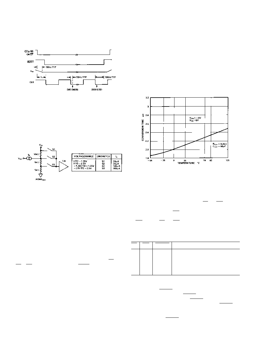
INTERNAL CLOCK
Clock pulses are generated by the action of an internal current
source charging the external capacitor (CCLK) and this external
capacitor discharging through the external resistor (RCLK).
When a conversion is complete, this internal clock stops operat-
ing and the CLK pin goes to the DGND potential. Connections
for RCLK and CCLK are shown in the operating diagram of Fig-
ure 21. The nominal conversion time versus temperature for the
recommended RCLK and CCLK combination is shown in Figure
6. The internal clock provides a convenient clock source for the
AD7569/AD7669. Due to process variations, the actual operat-
ing frequency for this RCLK/CCLK combination can vary from
device to device by up to
±25%.
Figure 6. Conversion Time vs. Temperature for Internal
Clock Operation
DIGITAL INTERFACE
DAC Timing and Control—AD7569
Table II shows the truth table for DAC operation for the
AD7569. The part contains an 8-bit DAC register, which is
loaded from the data bus under control of CS and WR. The
data contained in the DAC register determines the analog out-
put from the DAC. The WR input is an edge-triggered input,
and data is transferred into the DAC register on the rising edge
of WR. Holding CS and WR low does not make the DAC regis-
ter transparent.
Table II. AD7569 DAC Truth Table
CS
WR
RESET
DAC Function
H
DAC Register Unaffected
L
H
DAC Register Unaffected
L
g
H
DAC Register Updated
g
L
H
DAC Register Updated
X
L
DAC Register Loaded with All Zeros
L = Low State, H = High State, X = Don’t Care
The contents of the DAC register are reset to all 0s by an active
low pulse on the RESET line, and for the unipolar output ranges,
the output remains at 0 V after RESET returns high. For the bi-
polar output ranges, a low pulse on RESET causes the output to
go to negative full scale. In unipolar applications, the RESET line
can be used to ensure power-up to 0 V on the AD7569 DAC out-
put and is also useful when used as a zero override in system cali-
bration cycles. If the RESET input is connected to the system
At the end of conversion, the SAR contents are transferred to
the output latch, and the SAR is reset in readiness for a new
conversion. A single conversion lasts for 8 input clock cycles.
Figure 4. Operating Waveforms Using External Clock
ANALOG INPUT
The analog input of the AD7569/AD7669 feeds into an on-chip
track-and-hold amplifier. To accommodate different full-scale
ranges, the analog input signal is conditioned by a gain/offset
network that conditions all input ranges so the internal ADC al-
ways works with a 0 V to +1.25 V signal. As a result, the input
current on the VIN input varies with the input range selected as
shown in Figure 5.
Figure 5. Equivalent VIN Circuit
TRACK-AND-HOLD
The track-and-hold (T/H) amplifier on the analog input of the
AD7569/AD7669 allows the ADC to accurately convert an in-
put sine wave of 2.5 V peak-to-peak amplitude up to a fre-
quency of 200 kHz, the Nyquist frequency of the ADC when
operated at its maximum throughput rate of 400 kHz. This
maximum rate of conversion includes conversion time and time
between conversions. Because the input bandwidth of the T/H
amplifier is much larger than 200 kHz, the input signal should
be band-limited to avoid converting high-frequency noise
components.
The operation of this T/H amplifier is essentially transparent to
the user. The T/H amplifier goes from its tracking mode to its
hold mode at the start of conversion. This occurs when the
ADC receives a conversion start command from either ST or
CS
& RD. At the end of conversion (BUSY going high), the
T/H reverts back to tracking the input signal.
EXTERNAL CLOCK
The AD7569/AD7669 ADC can be used with its on-chip clock
or with an externally applied clock. When using an external
clock, the CLK input of the AD7569/AD7669 may be driven
directly from 74HC, 4000B series buffers (such as 4049) or
from TTL buffers. When conversion is complete, the internal
clock is disabled. The external clock can continue to run be-
tween conversions without being disabled. The mark/space ratio
of the external clock can vary from 70/30 to 30/70.
相关PDF资料 |
PDF描述 |
|---|---|
| D38999/20WD97PN | CONN RCPT 12POS WALL MNT W/PINS |
| AD6620ASZ-REEL | IC DGTL RCVR DUAL 67MSPS 80-PQFP |
| 6274291-2 | CONN JACK VERT PCB 75 OHM BNC |
| AD7669JNZ | IC I/O PORT 8BIT ANLG 28DIP |
| D38999/24FF11PA | CONN RCPT 11POS JAM NUT W/PINS |
相关代理商/技术参数 |
参数描述 |
|---|---|
| AD7569BN | 制造商:Analog Devices 功能描述:Data Acquisition System Single ADC Single DAC 8-Bit 24-Pin PDIP 制造商:Rochester Electronics LLC 功能描述:8-BIT CMOS I/O PORT IC - Bulk |
| AD7569BNZ | 功能描述:IC I/O PORT 8BIT ANALOG 24DIP RoHS:是 类别:集成电路 (IC) >> 接口 - 专用 系列:LC²MOS 特色产品:NXP - I2C Interface 标准包装:1 系列:- 应用:2 通道 I²C 多路复用器 接口:I²C,SM 总线 电源电压:2.3 V ~ 5.5 V 封装/外壳:16-TSSOP(0.173",4.40mm 宽) 供应商设备封装:16-TSSOP 包装:剪切带 (CT) 安装类型:表面贴装 产品目录页面:825 (CN2011-ZH PDF) 其它名称:568-1854-1 |
| AD7569BQ | 功能描述:IC I/O PORT 8BIT ANLG 24-CDIP RoHS:否 类别:集成电路 (IC) >> 接口 - 专用 系列:LC²MOS 特色产品:NXP - I2C Interface 标准包装:1 系列:- 应用:2 通道 I²C 多路复用器 接口:I²C,SM 总线 电源电压:2.3 V ~ 5.5 V 封装/外壳:16-TSSOP(0.173",4.40mm 宽) 供应商设备封装:16-TSSOP 包装:剪切带 (CT) 安装类型:表面贴装 产品目录页面:825 (CN2011-ZH PDF) 其它名称:568-1854-1 |
| AD7569BR | 功能描述:IC I/O PORT 8BIT ANLG 24-SOIC RoHS:否 类别:集成电路 (IC) >> 接口 - 专用 系列:LC²MOS 标准包装:3,000 系列:- 应用:PDA,便携式音频/视频,智能电话 接口:I²C,2 线串口 电源电压:1.65 V ~ 3.6 V 封装/外壳:24-WQFN 裸露焊盘 供应商设备封装:24-QFN 裸露焊盘(4x4) 包装:带卷 (TR) 安装类型:表面贴装 产品目录页面:1015 (CN2011-ZH PDF) 其它名称:296-25223-2 |
| AD7569BR-REEL | 功能描述:Analog I/O Interface 24-SOIC 制造商:analog devices inc. 系列:LC2MOS 包装:带卷(TR) 零件状态:上次购买时间 应用:模拟 I/O 接口:总线 电压 - 电源:4.75 V ~ 5.25 V 封装/外壳:24-SOIC(0.295",7.50mm 宽) 供应商器件封装:24-SOIC 安装类型:表面贴装 标准包装:1 |
发布紧急采购,3分钟左右您将得到回复。