- 您现在的位置:买卖IC网 > PDF目录11767 > AD7569AQ (Analog Devices Inc)IC I/O PORT 8BIT ANLG 24-CDIP PDF资料下载
参数资料
| 型号: | AD7569AQ |
| 厂商: | Analog Devices Inc |
| 文件页数: | 9/20页 |
| 文件大小: | 0K |
| 描述: | IC I/O PORT 8BIT ANLG 24-CDIP |
| 标准包装: | 15 |
| 系列: | LC²MOS |
| 应用: | 模拟 I/O |
| 接口: | 总线 |
| 电源电压: | 4.75 V ~ 5.25 V |
| 封装/外壳: | 24-CDIP(0.300",7.62mm) |
| 供应商设备封装: | 24-CDIP |
| 包装: | 管件 |
| 安装类型: | 通孔 |
AD7569/AD7669
–17–
REV. B
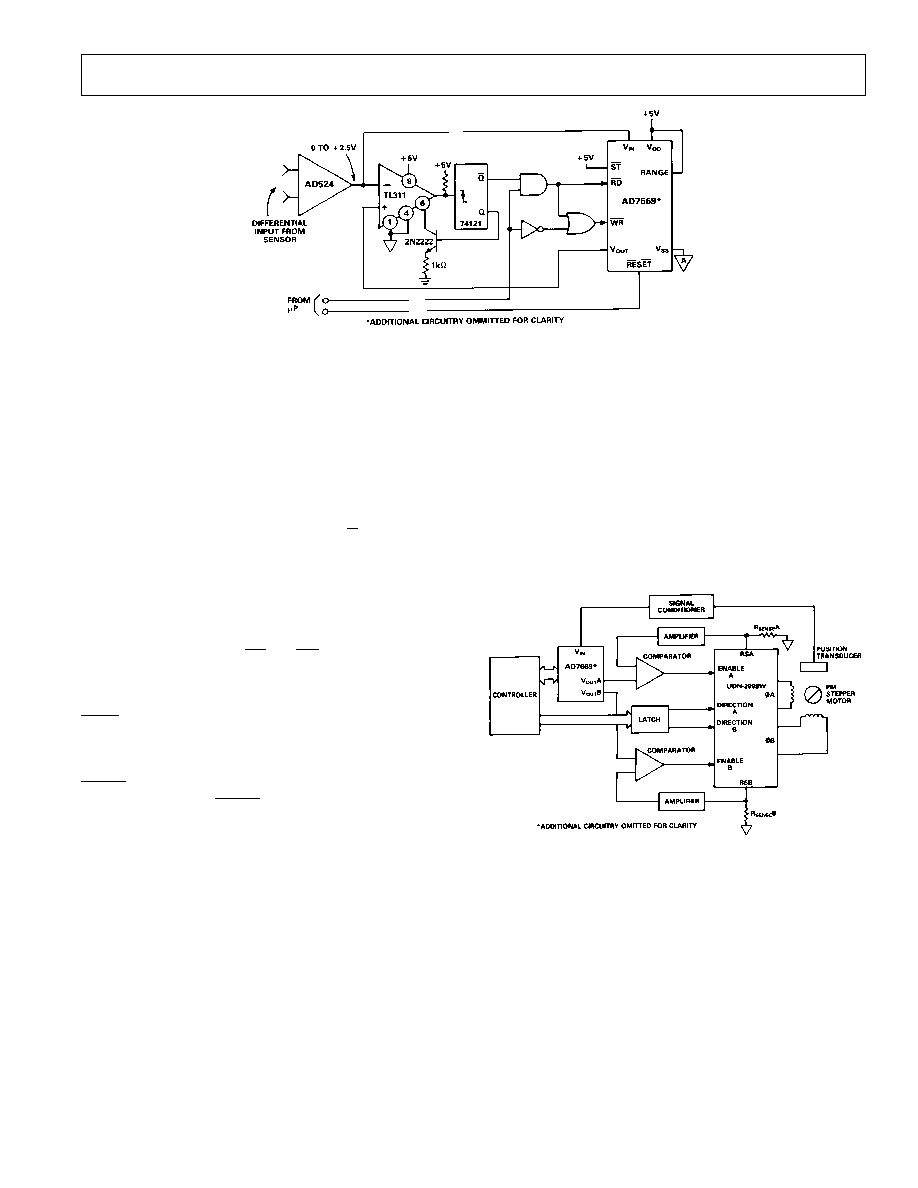
Figure 25. Peak-Reading A/D Converter
head (or motor) is monitored. The closed-loop system allows an
error between the desired position and the actual position to be
monitored and corrected. The correction is achieved by adjust-
ing the ratio of the phase currents in the motor windings until
the required head position is reached.
The AD7669 is ideally suited for the closed-loop microstepping
technique with its on-chip dual DACs for positioning the disk
drive head, and onboard ADC for monitoring the position of the
head. A generalized circuit for a closed-loop microstepping sys-
tem is shown in Figure 26. The DAC waveforms are shown in
Figure 27, along with the direction information for clockwise ro-
tation supplied by the controller.
Figure 26. Typical Closed-Loop Microstepping Circuit with
the AD7669
The AD7669 is used in the unipolar 0 V to +2.5 V configura-
tion. This allows the circuit of Figure 26 to be completely uni-
polar (+5 V, +12 V supplies); no negative power supplies are
required. The power output stage is a dual H-Bridge device
such as the UDN-2998W from Sprague Electric. The phase
currents in both windings are detected by means of the small
value sense resistors, RSA and RSB, in series with the windings.
The voltage developed across these resistors is amplified and
compared with the respective DAC output voltage. The com-
parators in turn chop the phase winding current. The ADC
completes the feedback path by converting information from a
suitable transducer for analysis by the controller.
PEAK DETECTION—AD7569
The circuit of Figure 25 shows a peak-reading A/D converter,
which is useful in such applications as monitoring flow rates,
temperature, pressure, etc. The circuit ensures that a peak will
not be missed while at the same time does not require the mi-
croprocessor to frequently monitor the data. The peak value is
stored in the A/D converter and can be read at any time.
The gain on the AD524 is adjusted to yield a 0 V to +2.5 V out-
put. When the input signal exceeds the current stored value, the
output of the TL311 goes low, triggering the Q output of the
74121. This low-going pulse starts a conversion on the AD7569
ADC, and at the end of conversion latches the result into the
DAC. This pulse must be at least 120 ns greater than the con-
version time of the ADC. The Q output is used to drive the
strobe input of the TL311, resetting the TL311 output high in
readiness for another conversion.
The additional gates on the RD and WR inputs are to allow the
data to be read by the microprocessor while at the same time
ensuring that the DAC is not updated when the microprocessor
reads the data. It may be necessary to monitor the AD7569
BUSY
line to ensure that a processor READ is not attempted
while the AD7569 is in the middle of a conversion. The READ
pulse width from the processor must be less than 1
s to ensure
correct data is read from the ADC. A low-going pulse on the
RESET
line resets the DAC output to 0 V and starts a new “peak-
detection” period. This RESET pulse must also be less than 1
s.
DISK DRIVE APPLICATION—AD7669
Closed-Loop Microstepping
Microstepping is a popular technique in low density disk drives
(both floppy and hard disk) that allows higher positional resolu-
tion of the disk drive head over that obtainable from a full- step
driven stepper motor. Typically, a two-phase stepper motor has
its phase currents driven with a sine-cosine relationship. These
cosinusoidal signals are generated by two DACs driven with the
appropriate data. The resolution of the DACs determines the
number of microsteps into which each full step can be divided.
For example, with a 1.8
° full-step motor and a 4-bit DAC, a
microstep size of 0.11
° (1.8°/(2n)) is obtainable.
The microstepping technique improves the positioning resolu-
tion possible in any control application; however, the positional
accuracy can be significantly worse than that offered by the
original full-step accuracy specification due to load torque effects.
To ensure that the increased resolution is usable, it is necessary
to use a closed-loop system where the position of the disk drive
相关PDF资料 |
PDF描述 |
|---|---|
| D38999/20WD97PN | CONN RCPT 12POS WALL MNT W/PINS |
| AD6620ASZ-REEL | IC DGTL RCVR DUAL 67MSPS 80-PQFP |
| 6274291-2 | CONN JACK VERT PCB 75 OHM BNC |
| AD7669JNZ | IC I/O PORT 8BIT ANLG 28DIP |
| D38999/24FF11PA | CONN RCPT 11POS JAM NUT W/PINS |
相关代理商/技术参数 |
参数描述 |
|---|---|
| AD7569BN | 制造商:Analog Devices 功能描述:Data Acquisition System Single ADC Single DAC 8-Bit 24-Pin PDIP 制造商:Rochester Electronics LLC 功能描述:8-BIT CMOS I/O PORT IC - Bulk |
| AD7569BNZ | 功能描述:IC I/O PORT 8BIT ANALOG 24DIP RoHS:是 类别:集成电路 (IC) >> 接口 - 专用 系列:LC²MOS 特色产品:NXP - I2C Interface 标准包装:1 系列:- 应用:2 通道 I²C 多路复用器 接口:I²C,SM 总线 电源电压:2.3 V ~ 5.5 V 封装/外壳:16-TSSOP(0.173",4.40mm 宽) 供应商设备封装:16-TSSOP 包装:剪切带 (CT) 安装类型:表面贴装 产品目录页面:825 (CN2011-ZH PDF) 其它名称:568-1854-1 |
| AD7569BQ | 功能描述:IC I/O PORT 8BIT ANLG 24-CDIP RoHS:否 类别:集成电路 (IC) >> 接口 - 专用 系列:LC²MOS 特色产品:NXP - I2C Interface 标准包装:1 系列:- 应用:2 通道 I²C 多路复用器 接口:I²C,SM 总线 电源电压:2.3 V ~ 5.5 V 封装/外壳:16-TSSOP(0.173",4.40mm 宽) 供应商设备封装:16-TSSOP 包装:剪切带 (CT) 安装类型:表面贴装 产品目录页面:825 (CN2011-ZH PDF) 其它名称:568-1854-1 |
| AD7569BR | 功能描述:IC I/O PORT 8BIT ANLG 24-SOIC RoHS:否 类别:集成电路 (IC) >> 接口 - 专用 系列:LC²MOS 标准包装:3,000 系列:- 应用:PDA,便携式音频/视频,智能电话 接口:I²C,2 线串口 电源电压:1.65 V ~ 3.6 V 封装/外壳:24-WQFN 裸露焊盘 供应商设备封装:24-QFN 裸露焊盘(4x4) 包装:带卷 (TR) 安装类型:表面贴装 产品目录页面:1015 (CN2011-ZH PDF) 其它名称:296-25223-2 |
| AD7569BR-REEL | 功能描述:Analog I/O Interface 24-SOIC 制造商:analog devices inc. 系列:LC2MOS 包装:带卷(TR) 零件状态:上次购买时间 应用:模拟 I/O 接口:总线 电压 - 电源:4.75 V ~ 5.25 V 封装/外壳:24-SOIC(0.295",7.50mm 宽) 供应商器件封装:24-SOIC 安装类型:表面贴装 标准包装:1 |
发布紧急采购,3分钟左右您将得到回复。