- 您现在的位置:买卖IC网 > PDF目录11767 > AD7569BNZ (Analog Devices Inc)IC I/O PORT 8BIT ANALOG 24DIP PDF资料下载
参数资料
| 型号: | AD7569BNZ |
| 厂商: | Analog Devices Inc |
| 文件页数: | 4/20页 |
| 文件大小: | 0K |
| 描述: | IC I/O PORT 8BIT ANALOG 24DIP |
| 标准包装: | 15 |
| 系列: | LC²MOS |
| 应用: | 模拟 I/O |
| 接口: | 总线 |
| 电源电压: | 4.75 V ~ 5.25 V |
| 封装/外壳: | 24-DIP(0.300",7.62mm) |
| 供应商设备封装: | 24-PDIP |
| 包装: | 管件 |
| 安装类型: | 通孔 |
–12–
REV. B
AD7569/AD7669
MODE 1 INTERFACE
The timing diagram for the first mode is shown in Figure 10. It
can be used in digital signal processing and other applications
where precise sampling in time is required. In these applica-
tions, it is important that the signal sampling occurs at exactly
equal intervals to minimize errors due to sampling uncertainty
or jitter. In these cases, the ST line is driven by a timer or some
precise clock source.
The falling edge of the ST pulse starts conversion and drives the
AD7569/AD7669 track-and-hold amplifier into its hold mode.
BUSY
stays low for the duration of conversion and returns high
at the end of conversion and the track-and hold amplifier reverts
to its tracking mode on this rising edge of BUSY. The INT line
can be used to interrupt the microprocessor. A READ to the
AD7569/AD7669 address accesses the data, and the INT line is
reset on the rising edge of CS or RD. Alternatively, the INT can
be used to trigger a pulse that drives the CS and RD and places
the data into a FIFO or buffer memory. The microprocessor can
then read a batch of data from the FIFO or buffer memory at
some convenient time. The ST input should not be high when
RD
is brought low; otherwise, the part will not operate correctly
in this mode.
It is important, especially in systems where the conversion start
(ST pulse) is asynchronous to the microprocessor, that a READ
does not occur during a conversion. Trying to read data from
the device during a conversion can cause errors to the conver-
sion in progress. Also, pulsing the ST line a second time before
conversion ends should be avoided since it too can cause errors
in the conversion result. In applications where precise sampling
is not critical, the ST pulse can be generated from a micropro-
cessor WR or RD line gated with a decoded address (different
from AD7569/AD7669 CS address).
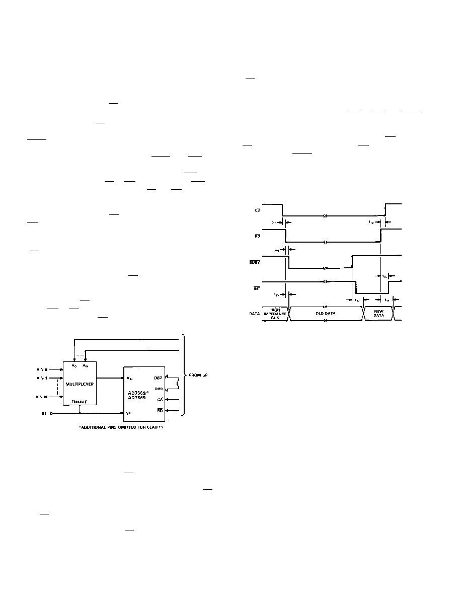
Figure 11. Multichannel Inputs
This interface mode is also useful in applications where a num-
ber of input channels are required to be converted by the ADC.
Figure 11 shows the circuit configuration for such an applica-
tion. The signal that drives the ST input of the AD7569/
AD7669 is also used to drive the ENABLE input of the multi-
plexer. The multiplexer is enabled on the rising edge of the ST
pulse while the input signal is held on the falling edge; therefore,
the signal must have settled to within 8 bits over the duration of
this ST pulse. The settling time, including tON (ENABLE) of
the multiplexer plus the T/H acquisition time (typically 200 ns),
thus determines the width of the ST pulse. This is suited to ap-
plications where a number of input channels needs to be succes-
sively sampled or scanned.
MODE 2 INTERFACE
The second interface mode is intended for use with micropro-
cessors, which can be forced into a WAIT state for at least 2
s.
The ST line of the AD7569/AD7669 must be hardwired high to
achieve this mode. The microprocessor starts a conversion and
is halted until the result of the conversion is read from the con-
verter. Conversion is initiated by executing a memory READ to
the AD7569/AD7669 address, bringing CS and RD low. BUSY
subsequently goes low (forcing the microprocessor READY or
WAIT input low), placing the microprocessor into a WAIT
state. The input signal is held on the falling edge of RD (assum-
ing CS is already low or is coincident with RD). When the con-
version is complete (BUSY goes high), the processor completes
the memory READ and acquires the newly converted data.
While conversion is in progress, the ADC places old data (from
the previous conversion) on the data bus. The timing diagram
for this interface is shown in Figure 12.
Figure 12. ADC Mode 2 Interface Timing
The major advantage of this interface is that it allows the micro-
processor to start conversion, WAIT, and then READ data with
a single READ instruction. The user does not have to worry
about servicing interrupts or ensuring that software delays are
long enough to avoid reading during conversion. The fast con-
version time of the ADC ensures that for many microprocessors,
the processor is not placed in a WAIT state for an excessive
amount of time.
DIGITAL SIGNAL PROCESSING APPLICATIONS
In Digital Signal Processing (DSP) application areas such as
voice recognition, echo cancellation and adaptive filtering, the
dynamic characteristics (SNR, Harmonic Distortion, Intermod-
ulation Distortion) of both the ADC and DAC are critical. The
AD7569/AD7669 is specified dynamically as well as with stan-
dard dc specifications. Because the track/hold amplifier has a
wide bandwidth, an antialiasing filter should be placed on the
VIN input to avoid aliasing of high-frequency noise back into the
band of interest.
The dynamic performance of the ADC is evaluated by applying a
sine-wave signal of very low distortion to the VIN input, which is
sampled at a 409.6 kHz sampling rate. A Fast Fourier Transform
(FFT) plot or Histogram plot is then generated from which SNR,
harmonic distortion and dynamic differential nonlinearity data
can be obtained. For the DAC, the codes for an ideal sine wave
are stored in PROM and loaded down to the DAC. The output
spectrum is analyzed, using a spectrum analyzer to evaluate SNR
相关PDF资料 |
PDF描述 |
|---|---|
| 5413515-9 | CONN JACK BNC RT ANG 50 OHM 30AU |
| AD7669JRZ | IC I/O PORT 8BIT ANLG 28SOIC |
| AD7569BRZ | IC I/O PORT 8BIT ANALOG 24SOIC |
| PIC16F723A-I/SP | MCU PIC 7KB FLASH XLP 28-SPDIP |
| PIC16C505-04/SL | IC MCU OTP 1KX12 14SOIC |
相关代理商/技术参数 |
参数描述 |
|---|---|
| AD7569BQ | 功能描述:IC I/O PORT 8BIT ANLG 24-CDIP RoHS:否 类别:集成电路 (IC) >> 接口 - 专用 系列:LC²MOS 特色产品:NXP - I2C Interface 标准包装:1 系列:- 应用:2 通道 I²C 多路复用器 接口:I²C,SM 总线 电源电压:2.3 V ~ 5.5 V 封装/外壳:16-TSSOP(0.173",4.40mm 宽) 供应商设备封装:16-TSSOP 包装:剪切带 (CT) 安装类型:表面贴装 产品目录页面:825 (CN2011-ZH PDF) 其它名称:568-1854-1 |
| AD7569BR | 功能描述:IC I/O PORT 8BIT ANLG 24-SOIC RoHS:否 类别:集成电路 (IC) >> 接口 - 专用 系列:LC²MOS 标准包装:3,000 系列:- 应用:PDA,便携式音频/视频,智能电话 接口:I²C,2 线串口 电源电压:1.65 V ~ 3.6 V 封装/外壳:24-WQFN 裸露焊盘 供应商设备封装:24-QFN 裸露焊盘(4x4) 包装:带卷 (TR) 安装类型:表面贴装 产品目录页面:1015 (CN2011-ZH PDF) 其它名称:296-25223-2 |
| AD7569BR-REEL | 功能描述:Analog I/O Interface 24-SOIC 制造商:analog devices inc. 系列:LC2MOS 包装:带卷(TR) 零件状态:上次购买时间 应用:模拟 I/O 接口:总线 电压 - 电源:4.75 V ~ 5.25 V 封装/外壳:24-SOIC(0.295",7.50mm 宽) 供应商器件封装:24-SOIC 安装类型:表面贴装 标准包装:1 |
| AD7569BRZ | 功能描述:IC I/O PORT 8BIT ANALOG 24SOIC RoHS:是 类别:集成电路 (IC) >> 接口 - 专用 系列:LC²MOS 特色产品:NXP - I2C Interface 标准包装:1 系列:- 应用:2 通道 I²C 多路复用器 接口:I²C,SM 总线 电源电压:2.3 V ~ 5.5 V 封装/外壳:16-TSSOP(0.173",4.40mm 宽) 供应商设备封装:16-TSSOP 包装:剪切带 (CT) 安装类型:表面贴装 产品目录页面:825 (CN2011-ZH PDF) 其它名称:568-1854-1 |
| AD7569JN | 功能描述:IC I/O PORT 8BIT ANLG 24-DIP RoHS:否 类别:集成电路 (IC) >> 接口 - 专用 系列:LC²MOS 标准包装:3,000 系列:- 应用:PDA,便携式音频/视频,智能电话 接口:I²C,2 线串口 电源电压:1.65 V ~ 3.6 V 封装/外壳:24-WQFN 裸露焊盘 供应商设备封装:24-QFN 裸露焊盘(4x4) 包装:带卷 (TR) 安装类型:表面贴装 产品目录页面:1015 (CN2011-ZH PDF) 其它名称:296-25223-2 |
发布紧急采购,3分钟左右您将得到回复。