- 您现在的位置:买卖IC网 > PDF目录11767 > AD7569BNZ (Analog Devices Inc)IC I/O PORT 8BIT ANALOG 24DIP PDF资料下载
参数资料
| 型号: | AD7569BNZ |
| 厂商: | Analog Devices Inc |
| 文件页数: | 6/20页 |
| 文件大小: | 0K |
| 描述: | IC I/O PORT 8BIT ANALOG 24DIP |
| 标准包装: | 15 |
| 系列: | LC²MOS |
| 应用: | 模拟 I/O |
| 接口: | 总线 |
| 电源电压: | 4.75 V ~ 5.25 V |
| 封装/外壳: | 24-DIP(0.300",7.62mm) |
| 供应商设备封装: | 24-PDIP |
| 包装: | 管件 |
| 安装类型: | 通孔 |
–14–
REV. B
AD7569/AD7669
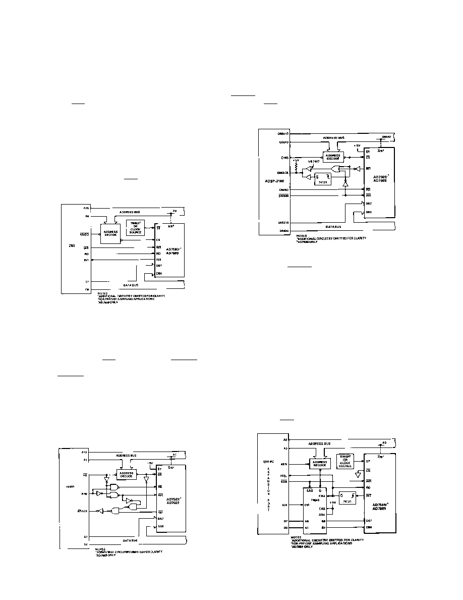
AD7569/AD7669—ADSP-2100 INTERFACE
Figure 19 shows a typical interface to the DSP processor, the
ADSP-2100. The ADC is in the Mode 2 interface mode, which
means that the ADSP-2100 is halted during conversion. This is
achieved using the decoded address output. This is gated with
DMWR
to ensure that it halts the processor for READ instruc-
tions only. INT going low at the end of conversion releases the
processor and allows it to finish off the READ instruction.
Figure 19. AD7569/AD7669 to ADSP-2100 Interface
Because the instruction cycle of the ADSP-2100 is so fast
(125 ns cycle), the DMWR pulse also has to be stretched also
for write cycles. This is achieved using the 74121, which gener-
ates a pulse that is fed back to DMACK. The duration of this
pulse determines how long the ADSP-2100 write cycle is
stretched. The buffers driving the DMACK line must have
open-collector outputs. Writing data to the relevant AD7569/
AD7669 DAC is achieved using a single instruction, <DM
(addr) = MRO>, where addr is the decoded address of that
DAC, and MRO contains the data to be loaded to the DAC reg-
ister. Data is read from the ADC also, using a single instruction
<MRO = DM (addr)>, where the conversion result is placed in
the MRO data register.
AD7569/AD7669—IBM PC* INTERFACE
The AD7569/AD7669 is ideal for implementing an analog in-
put/output port for the IBM PC. Figure 20 shows an interface
that realizes this function. The ADC is configured in the Mode
1 interface mode, and conversions are initiated using a precise
clock source for equidistant sampling intervals. At the end of
conversion, the INT line goes low, and the 74121 generates
Figure 20. AD7569/AD7669 to IBM PC Interface
*IBM PC is a trademark of International Business Machines Corp.
INTERFACING THE AD7569/AD7669
AD7569/AD7669—Z80 INTERFACE
Figure 17 shows a typical interface to the Z80 microprocessor.
The ADC is configured for operation in the Mode 1 interface
mode. A precise timer or clock source starts conversion in appli-
cations requiring equidistant sampling intervals. The scheme
used, whereby INT of the AD7569/AD7669 generates an inter-
rupt on the Z80, is limited in that it does not allow the ADC to
be sampled at the maximum rate. This is because the time be-
tween samples has to be long enough to allow the Z80 to service
its interrupt and read data from the ADC. To overcome this,
some buffer memory or FIFO could be placed between the
AD7569/AD7669 and the Z80. Writing data to the relevant
AD7569/AD7669 DAC simply consists of a <LD (nn), A> in-
struction where nn is the decoded address for that DAC. Read-
ing data from the ADC, after an INT has been received,
consists of a < LDA, (nn)> instruction.
Figure 17. AD7569/AD7669 to Z80 Interface
AD7569/AD7669—68008 INTERFACE
A typical interface to the 68008 is shown in Figure 18. In this
case, the ADC is configured in the Mode 2 interface mode. This
means that the one read instruction starts conversion and reads
the data. The read cycle is stretched out over the entire conver-
sion period by taking the INT line back into the DTACK input
of the 68008. The additional gates are required so the 68008
receives a DTACK when the processor is writing data to the
AD7569/AD7669. In this case, there are no wait states intro-
duced into the write cycle. Writing data to the relevant AD7569/
AD7669 DAC consists of a <MOVE.B Dn, addr> where Dn is
the data register, which contains the data to be loaded to that
DAC, and addr is the decoded address for the DAC. Data is
read from the ADC using a <MOVE.B addr,Dn> with the con-
version result placed in register Dn.
Figure 18. AD7569/AD7669 to 68008 Interface
相关PDF资料 |
PDF描述 |
|---|---|
| 5413515-9 | CONN JACK BNC RT ANG 50 OHM 30AU |
| AD7669JRZ | IC I/O PORT 8BIT ANLG 28SOIC |
| AD7569BRZ | IC I/O PORT 8BIT ANALOG 24SOIC |
| PIC16F723A-I/SP | MCU PIC 7KB FLASH XLP 28-SPDIP |
| PIC16C505-04/SL | IC MCU OTP 1KX12 14SOIC |
相关代理商/技术参数 |
参数描述 |
|---|---|
| AD7569BQ | 功能描述:IC I/O PORT 8BIT ANLG 24-CDIP RoHS:否 类别:集成电路 (IC) >> 接口 - 专用 系列:LC²MOS 特色产品:NXP - I2C Interface 标准包装:1 系列:- 应用:2 通道 I²C 多路复用器 接口:I²C,SM 总线 电源电压:2.3 V ~ 5.5 V 封装/外壳:16-TSSOP(0.173",4.40mm 宽) 供应商设备封装:16-TSSOP 包装:剪切带 (CT) 安装类型:表面贴装 产品目录页面:825 (CN2011-ZH PDF) 其它名称:568-1854-1 |
| AD7569BR | 功能描述:IC I/O PORT 8BIT ANLG 24-SOIC RoHS:否 类别:集成电路 (IC) >> 接口 - 专用 系列:LC²MOS 标准包装:3,000 系列:- 应用:PDA,便携式音频/视频,智能电话 接口:I²C,2 线串口 电源电压:1.65 V ~ 3.6 V 封装/外壳:24-WQFN 裸露焊盘 供应商设备封装:24-QFN 裸露焊盘(4x4) 包装:带卷 (TR) 安装类型:表面贴装 产品目录页面:1015 (CN2011-ZH PDF) 其它名称:296-25223-2 |
| AD7569BR-REEL | 功能描述:Analog I/O Interface 24-SOIC 制造商:analog devices inc. 系列:LC2MOS 包装:带卷(TR) 零件状态:上次购买时间 应用:模拟 I/O 接口:总线 电压 - 电源:4.75 V ~ 5.25 V 封装/外壳:24-SOIC(0.295",7.50mm 宽) 供应商器件封装:24-SOIC 安装类型:表面贴装 标准包装:1 |
| AD7569BRZ | 功能描述:IC I/O PORT 8BIT ANALOG 24SOIC RoHS:是 类别:集成电路 (IC) >> 接口 - 专用 系列:LC²MOS 特色产品:NXP - I2C Interface 标准包装:1 系列:- 应用:2 通道 I²C 多路复用器 接口:I²C,SM 总线 电源电压:2.3 V ~ 5.5 V 封装/外壳:16-TSSOP(0.173",4.40mm 宽) 供应商设备封装:16-TSSOP 包装:剪切带 (CT) 安装类型:表面贴装 产品目录页面:825 (CN2011-ZH PDF) 其它名称:568-1854-1 |
| AD7569JN | 功能描述:IC I/O PORT 8BIT ANLG 24-DIP RoHS:否 类别:集成电路 (IC) >> 接口 - 专用 系列:LC²MOS 标准包装:3,000 系列:- 应用:PDA,便携式音频/视频,智能电话 接口:I²C,2 线串口 电源电压:1.65 V ~ 3.6 V 封装/外壳:24-WQFN 裸露焊盘 供应商设备封装:24-QFN 裸露焊盘(4x4) 包装:带卷 (TR) 安装类型:表面贴装 产品目录页面:1015 (CN2011-ZH PDF) 其它名称:296-25223-2 |
发布紧急采购,3分钟左右您将得到回复。