- 您现在的位置:买卖IC网 > PDF目录11767 > AD7569JPZ (Analog Devices Inc)IC I/O PORT 8BIT ANLG 28PLCC PDF资料下载
参数资料
| 型号: | AD7569JPZ |
| 厂商: | Analog Devices Inc |
| 文件页数: | 3/20页 |
| 文件大小: | 0K |
| 描述: | IC I/O PORT 8BIT ANLG 28PLCC |
| 标准包装: | 39 |
| 系列: | LC²MOS |
| 应用: | 模拟 I/O |
| 接口: | 总线 |
| 电源电压: | 4.75 V ~ 5.25 V |
| 封装/外壳: | 28-LCC(J 形引线) |
| 供应商设备封装: | 28-PLCC(11.51x11.51) |
| 包装: | 管件 |
| 安装类型: | 表面贴装 |
AD7569/AD7669
–11–
REV. B
RESET
line, the DAC output resets to 0 V when the entire
system is reset. Figure 7 shows the input control logic for the
AD7569 DAC; the write cycle timing diagram is shown in
Figure 8.
Figure 7. AD7569 DAC Input Control Logic
Figure 8. AD7569/AD7669 Write Cycle Timing Diagram
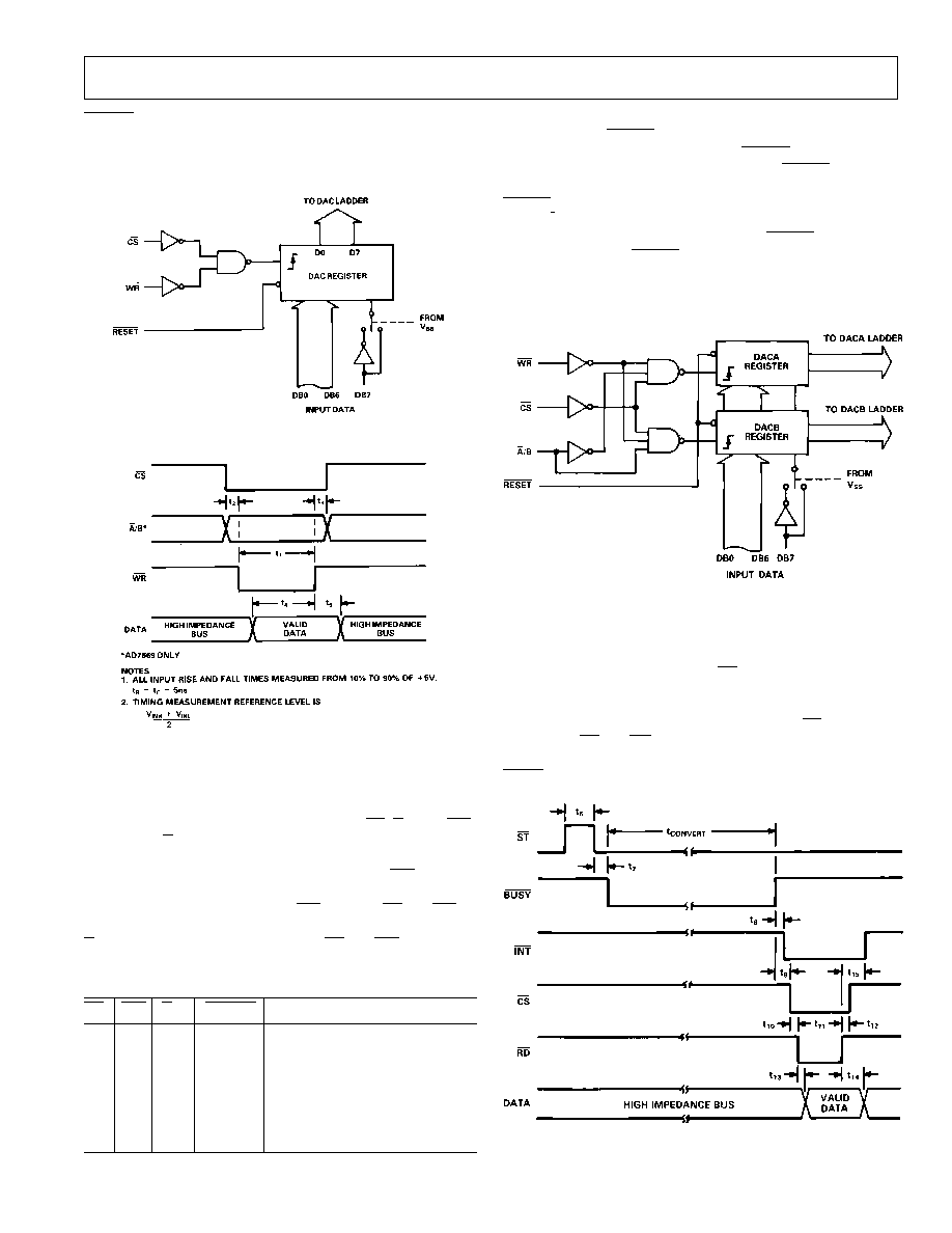
DAC Timing and Control—AD7669
Table III shows the truth table for the dual DAC operation of
the AD7669. The part contains two 8-bit DAC registers that are
loaded from the data bus under the control of CS, A/B and WR.
Address line A/B selects which DAC register the data is
loaded to. The data contained in the DAC registers determines
the analog output from the respective DACs. The WR input is
an edge-triggered input, and data is transferred into the selected
DAC register on the rising edge of WR. Holding CS and WR
low does not make the selected DAC register transparent. The
A
/B input should not be changed while CS and WR are low.
Table III. AD7669 DAC Truth Table
CS
WR
A
/B
RESET
DAC Function
H
X
H
DAC Registers Unaffected
L
g
L
H
DACA Register Updated
g
L
H
DACA Register Updated
L
g
H
DACB Register Updated
g
L
H
DACB Register Updated
X
L
DAC Registers Loaded with
All Zeros
L = Low State, H = High State, X = Don’t Care
The contents of the DAC registers are reset to all 0s by an active
low pulse on the RESET line, and for the unipolar output
ranges, the outputs remain at 0 V after RESET returns high.
For the bipolar output ranges, a low pulse on RESET causes the
outputs to go to negative full scale. In unipolar applications, the
RESET
line can be used to ensure power-up to 0 V on the
AD7669 DAC outputs and is also useful when used as a zero
override in system calibration cycles. If the RESET input is con-
nected to the system RESET line, then the DAC outputs reset
to 0 V when the entire system is reset. Figure 9 shows the DAC
input control logic for the AD7669, and the write cycle timing
diagram is shown in Figure 8.
Figure 9. AD7669 DAC Control Logic
ADC Timing and Control
The ADC on the AD7569/AD7669 is capable of two basic oper-
ating modes. In the first mode, the ST line is used to start con-
version and drive the track-and-hold into hold mode. At the end
of conversion, the track-and-hold returns to its tracking mode.
The second mode is achieved by hard-wiring the ST line high.
In this case, CS and RD start conversion, and the microproces-
sor is driven into a WAIT state for the duration of conversion by
BUSY
.
Figure 10. ADC Mode 1 Interface Timing
相关PDF资料 |
PDF描述 |
|---|---|
| AD7569JP | IC I/O PORT 8BIT ANLG 28-PLCC |
| PIC16LF1903-I/SP | MCU 7KB FLASH LCD DVR 28-SPDIP |
| AD7669JRZ-REEL | IC I/O PORT 8BIT ANLG 28SOIC |
| 5413515-8 | CONN JACK BNC RT ANG 50 OHM 30AU |
| AD7669ARZ-REEL | IC I/O PORT 8BIT ANALOG 28SOIC |
相关代理商/技术参数 |
参数描述 |
|---|---|
| AD7569JPZ-REEL | 功能描述:IC I/O PORT 8BIT ANLG 28PLCC RoHS:是 类别:集成电路 (IC) >> 接口 - 专用 系列:LC²MOS 特色产品:NXP - I2C Interface 标准包装:1 系列:- 应用:2 通道 I²C 多路复用器 接口:I²C,SM 总线 电源电压:2.3 V ~ 5.5 V 封装/外壳:16-TSSOP(0.173",4.40mm 宽) 供应商设备封装:16-TSSOP 包装:剪切带 (CT) 安装类型:表面贴装 产品目录页面:825 (CN2011-ZH PDF) 其它名称:568-1854-1 |
| AD7569JR | 制造商:Rochester Electronics LLC 功能描述:8-BIT CMOS I/O PORT IC - Bulk |
| AD7569JR-REEL | 制造商:Analog Devices 功能描述:Data Acquisition System Single ADC Single DAC 8-Bit 24-Pin SOIC W T/R |
| AD7569JRZ | 功能描述:IC I/O PORT 8BIT ANALOG 24-SOIC RoHS:是 类别:集成电路 (IC) >> 接口 - 专用 系列:LC²MOS 特色产品:NXP - I2C Interface 标准包装:1 系列:- 应用:2 通道 I²C 多路复用器 接口:I²C,SM 总线 电源电压:2.3 V ~ 5.5 V 封装/外壳:16-TSSOP(0.173",4.40mm 宽) 供应商设备封装:16-TSSOP 包装:剪切带 (CT) 安装类型:表面贴装 产品目录页面:825 (CN2011-ZH PDF) 其它名称:568-1854-1 |
| AD7569JRZ-REEL | 功能描述:IC I/O PORT 8BIT ANALOG 24SOIC RoHS:是 类别:集成电路 (IC) >> 接口 - 专用 系列:LC²MOS 标准包装:3,000 系列:- 应用:PDA,便携式音频/视频,智能电话 接口:I²C,2 线串口 电源电压:1.65 V ~ 3.6 V 封装/外壳:24-WQFN 裸露焊盘 供应商设备封装:24-QFN 裸露焊盘(4x4) 包装:带卷 (TR) 安装类型:表面贴装 产品目录页面:1015 (CN2011-ZH PDF) 其它名称:296-25223-2 |
发布紧急采购,3分钟左右您将得到回复。