- 您现在的位置:买卖IC网 > PDF目录11767 > AD7569JPZ (Analog Devices Inc)IC I/O PORT 8BIT ANLG 28PLCC PDF资料下载
参数资料
| 型号: | AD7569JPZ |
| 厂商: | Analog Devices Inc |
| 文件页数: | 8/20页 |
| 文件大小: | 0K |
| 描述: | IC I/O PORT 8BIT ANLG 28PLCC |
| 标准包装: | 39 |
| 系列: | LC²MOS |
| 应用: | 模拟 I/O |
| 接口: | 总线 |
| 电源电压: | 4.75 V ~ 5.25 V |
| 封装/外壳: | 28-LCC(J 形引线) |
| 供应商设备封装: | 28-PLCC(11.51x11.51) |
| 包装: | 管件 |
| 安装类型: | 表面贴装 |
–16–
REV. B
AD7569/AD7669
APPLYING THE AD7569/AD7669 ADC
The analog input on the AD7569/AD7669 accepts the same
four input ranges as the output ranges on the DAC. Whatever
output range is selected for the DAC also applies to the input
range of the ADC.
Although separate AGNDs exist for both the DAC and ADC to
minimize crosstalk, writing data to the DAC while the ADC is
performing a conversion may result in an incorrect conversion
from the ADC due to an interaction of currents between the
DAC and ADC. Therefore, to ensure correct operation of the
ADC, the DAC register should not be updated while the ADC
is converting.
UNIPOLAR OPERATION
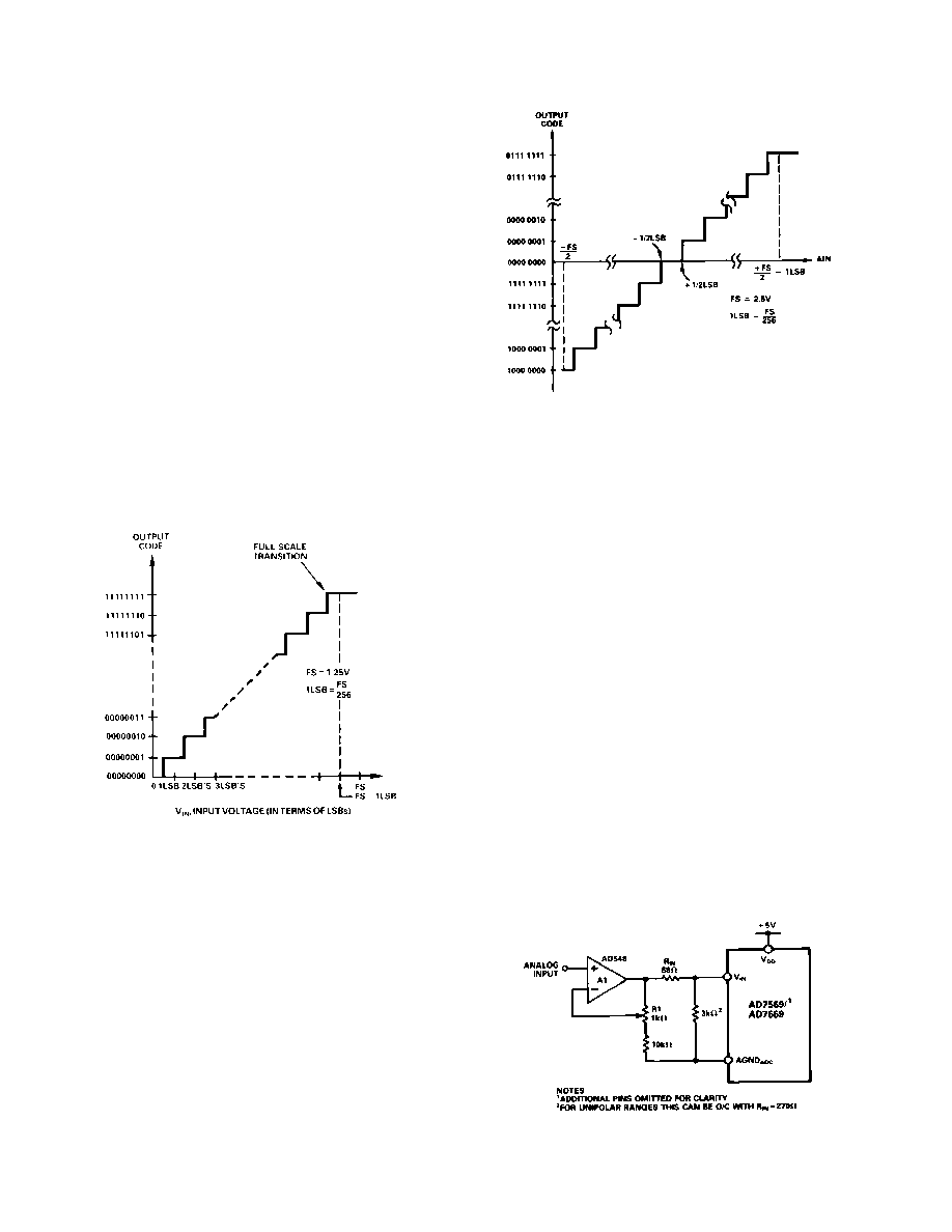
The circuit of Figure 21 shows the AD7569 configured for both
an input and output range of 0 V to +1.25 V (the AD7669 con-
figuration is similar). The nominal transfer characteristic for this
range is shown in Figure 22. The output code is Natural Binary
with 1 LSB = (1.25/256)V = 4.88 mV.
As before, to achieve the unipolar 0 V to +2.5 V input range,
VSS is connected to 0 V, and the RANGE input is tied to a logic
high. The nominal transfer characteristic is as in Figure 22 but,
in this case, 1 LSB = (2.5/256)V = 9.76 mV.
Figure 22. Nominal Transfer Characteristic for Unipolar
(0 V to +1.25 V) Operation
BIPOLAR OPERATION
The analog input of the AD7569/AD7669 ADC is configured
for bipolar inputs when VSS = –5 V. The output code provided
by the part is twos complement. Figure 23 shows the transfer
function for bipolar (–1.25 V to +1.25 V) operation. The LSB
size for this range is (2.5/256)V = 9.76 mV.
The transfer function for the –2.5 V to +2.5 V range is identical
to that of Figure 23, but now FS = 5 V and the LSB size is
(5/256)V = 19.5 mV.
ADC OFFSET AND FULL-SCALE ERROR ADJUSTMENT
In most Digital Signal Processing (DSP) applications, offset and
full-scale error have little or no effect on system performance. A
Figure 23. Nominal Transfer Characteristic for Bipolar
(–1.25 V to +1.25 V) Operation
typical example is a digital filter where an ac analog signal is
quantized by the ADC, digitally processed and recreated using
the DAC. In these types of applications, the offset error can be
eliminated by ac coupling the recreated signal. Full-scale error
effect is linear and does not cause problems as long as the input
signal is within the full dynamic range of the ADC. An impor-
tant parameter in DSP applications is Differential Nonlinearity,
and this is not affected by either offset or full-scale error.
In applications where absolute accuracy is important ADC off-
set and full-scale error can be adjusted to zero. Figure 24 shows
the additional components required for offset and full-scale er-
ror adjustment. Offset error must be adjusted before full-scale
error. Zero offset is achieved by adjusting the offset of the op
amp driving VIN (i.e., A1 in Figure 23). In unipolar applica-
tions, for zero offset error, apply 1/2 LSB at the analog input
and adjust the op amp offset voltage until the ADC output code
flickers between 0000 0000 and 0000 0001. For zero full-scale
error, apply an analog input of FS – 3/2 LSBs and adjust R1 un-
til the ADC output code flickers between 1111 1110 and 1111
1111.
In bipolar applications, to adjust for bipolar zero offset, apply
–1/2 LSB at the analog input and adjust the op amp offset volt-
age until the output code flickers between 1111 1111 and 0000
0000. For zero full-scale error, apply +FS/2 – 3/2 LSB at the
analog input and adjust R1 until the ADC output code flickers
between 0111 1110 and 0111 1111.
Figure 24. ADC Error Adjust Circuit
相关PDF资料 |
PDF描述 |
|---|---|
| AD7569JP | IC I/O PORT 8BIT ANLG 28-PLCC |
| PIC16LF1903-I/SP | MCU 7KB FLASH LCD DVR 28-SPDIP |
| AD7669JRZ-REEL | IC I/O PORT 8BIT ANLG 28SOIC |
| 5413515-8 | CONN JACK BNC RT ANG 50 OHM 30AU |
| AD7669ARZ-REEL | IC I/O PORT 8BIT ANALOG 28SOIC |
相关代理商/技术参数 |
参数描述 |
|---|---|
| AD7569JPZ-REEL | 功能描述:IC I/O PORT 8BIT ANLG 28PLCC RoHS:是 类别:集成电路 (IC) >> 接口 - 专用 系列:LC²MOS 特色产品:NXP - I2C Interface 标准包装:1 系列:- 应用:2 通道 I²C 多路复用器 接口:I²C,SM 总线 电源电压:2.3 V ~ 5.5 V 封装/外壳:16-TSSOP(0.173",4.40mm 宽) 供应商设备封装:16-TSSOP 包装:剪切带 (CT) 安装类型:表面贴装 产品目录页面:825 (CN2011-ZH PDF) 其它名称:568-1854-1 |
| AD7569JR | 制造商:Rochester Electronics LLC 功能描述:8-BIT CMOS I/O PORT IC - Bulk |
| AD7569JR-REEL | 制造商:Analog Devices 功能描述:Data Acquisition System Single ADC Single DAC 8-Bit 24-Pin SOIC W T/R |
| AD7569JRZ | 功能描述:IC I/O PORT 8BIT ANALOG 24-SOIC RoHS:是 类别:集成电路 (IC) >> 接口 - 专用 系列:LC²MOS 特色产品:NXP - I2C Interface 标准包装:1 系列:- 应用:2 通道 I²C 多路复用器 接口:I²C,SM 总线 电源电压:2.3 V ~ 5.5 V 封装/外壳:16-TSSOP(0.173",4.40mm 宽) 供应商设备封装:16-TSSOP 包装:剪切带 (CT) 安装类型:表面贴装 产品目录页面:825 (CN2011-ZH PDF) 其它名称:568-1854-1 |
| AD7569JRZ-REEL | 功能描述:IC I/O PORT 8BIT ANALOG 24SOIC RoHS:是 类别:集成电路 (IC) >> 接口 - 专用 系列:LC²MOS 标准包装:3,000 系列:- 应用:PDA,便携式音频/视频,智能电话 接口:I²C,2 线串口 电源电压:1.65 V ~ 3.6 V 封装/外壳:24-WQFN 裸露焊盘 供应商设备封装:24-QFN 裸露焊盘(4x4) 包装:带卷 (TR) 安装类型:表面贴装 产品目录页面:1015 (CN2011-ZH PDF) 其它名称:296-25223-2 |
发布紧急采购,3分钟左右您将得到回复。