参数资料
| 型号: | AD7606BSTZ-4 |
| 厂商: | Analog Devices Inc |
| 文件页数: | 15/36页 |
| 文件大小: | 0K |
| 描述: | IC DAS W/ADC 16BIT 4CH 64LQFP |
| 设计资源: | Layout Considerations for an Expandable Multichannel Simultaneous Sampling Data Acquisition System Based on AD7606 (CN0148) |
| 标准包装: | 1 |
| 类型: | 数据采集系统(DAS),ADC |
| 分辨率(位): | 16 b |
| 采样率(每秒): | 200k |
| 数据接口: | DSP,MICROWIRE?,并联,QSPI?,串行,SPI? |
| 电压电源: | 模拟和数字 |
| 电源电压: | 2.3 V ~ 5.25 V,4.75 V ~ 5.25 V |
| 工作温度: | -40°C ~ 85°C |
| 安装类型: | 表面贴装 |
| 封装/外壳: | 64-LQFP |
| 供应商设备封装: | 64-LQFP(10x10) |
| 包装: | 托盘 |
第1页第2页第3页第4页第5页第6页第7页第8页第9页第10页第11页第12页第13页第14页当前第15页第16页第17页第18页第19页第20页第21页第22页第23页第24页第25页第26页第27页第28页第29页第30页第31页第32页第33页第34页第35页第36页
AD7606/AD7606-6/AD7606-4
Data Sheet
Rev. C | Page 22 of 36
THEORY OF OPERATION
CONVERTER DETAILS
The AD7606/AD7606-6/AD7606-4 are data acquisition systems
that employ a high speed, low power, charge redistribution,
successive approximation analog-to-digital converter (ADC)
and allow the simultaneous sampling of eight/six/four analog input
channels. The analog inputs on the AD7606/AD7606-6/AD7606-4
can accept true bipolar input signals. The RANGE pin is used to
select either ±10 V or ±5 V as the input range. The AD7606/
AD7606-6/AD7606-4 operate from a single 5 V supply.
The AD7606/AD7606-6/AD7606-4 contain input clamp
protection, input signal scaling amplifiers, a second-order anti-
aliasing filter, track-and-hold amplifiers, an on-chip reference,
reference buffers, a high speed ADC, a digital filter, and high
speed parallel and serial interfaces. Sampling on the AD7606/
AD7606-6/AD7606-4 is controlled using the CONVST signals.
ANALOG INPUT
Analog Input Ranges
The AD7606/AD7606-6/AD7606-4 can handle true bipolar,
single-ended input voltages. The logic level on the RANGE pin
determines the analog input range of all analog input channels.
If this pin is tied to a logic high, the analog input range is ±10 V
for all channels. If this pin is tied to a logic low, the analog input
range is ±5 V for all channels. A logic change on this pin has an
immediate effect on the analog input range; however, there is
typically a settling time of approximately 80 s, in addition to
the normal acquisition time requirement. The recommended
practice is to hardwire the RANGE pin according to the desired
input range for the system signals.
During normal operation, the applied analog input voltage
should remain within the analog input range selected via the
RANGE pin. A RESET pulse must be applied after power up to
ensure the analog input channels are configured for the range
selected.
When in a power-down mode, it is recommended to tie the
analog inputs to GND. Per the Analog Input Clamp Protection
section, the overvoltage clamp protection is recommended for
use in transient overvoltage conditions and should not remain
active for extended periods. Stressing the analog inputs outside
of the conditions mentioned here may degrade the bipolar zero
code error and THD performance of the AD7606/AD7606-6/
AD7606-4.
Analog Input Impedance
The analog input impedance of the AD7606/AD7606-6/
AD7606-4 is 1 M. This is a fixed input impedance that does
not vary with the AD7606 sampling frequency. This high analog
input impedance eliminates the need for a driver amplifier in
front of the AD7606/AD7606-6/AD7606-4, allowing for direct
connection to the source or sensor. With the need for a driver
amplifier eliminated, bipolar supplies (which are often a source
of noise in a system) can be removed from the signal chain.
Analog Input Clamp Protection
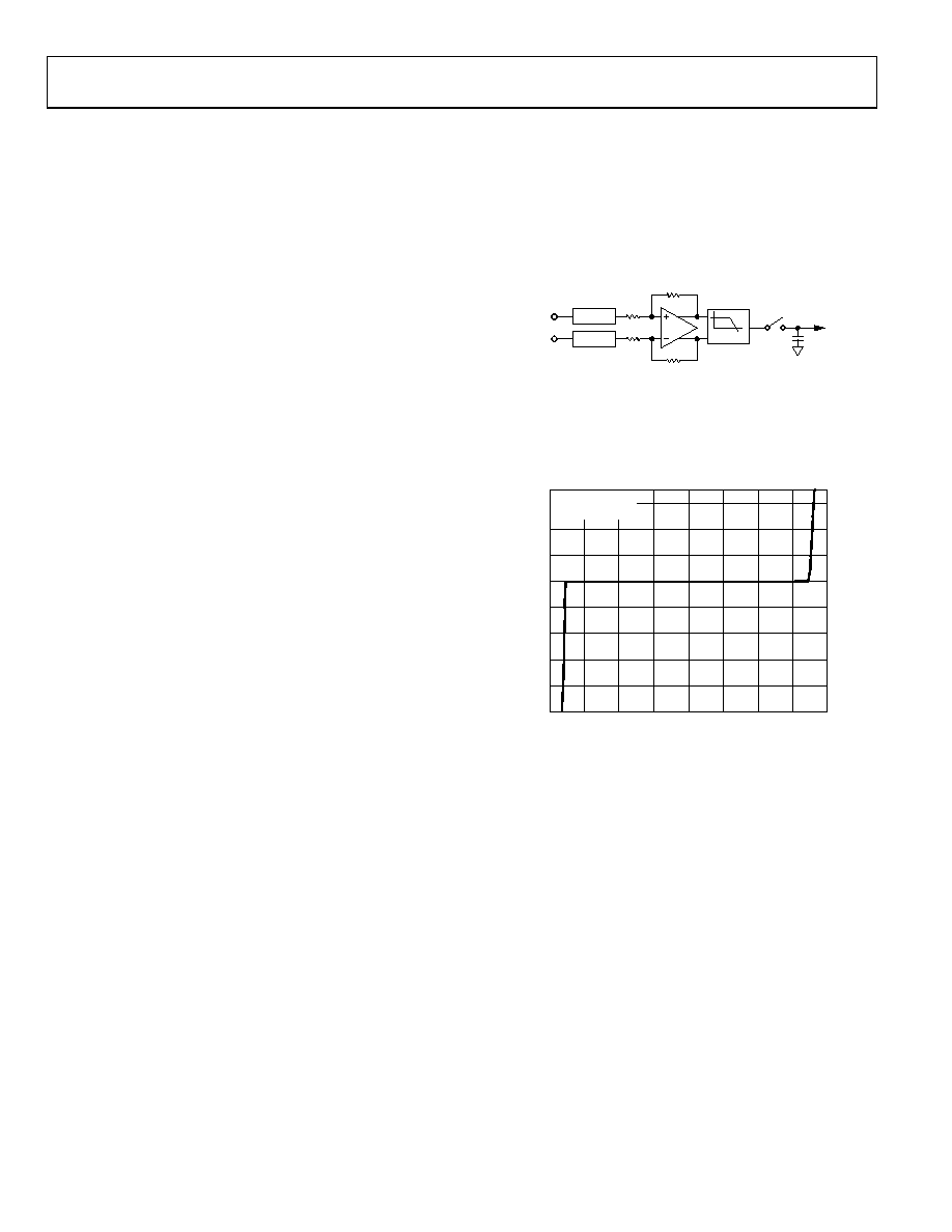
Figure 34 shows the analog input structure of the AD7606/
AD7606-6/AD7606-4. Each analog input of the AD7606/
AD7606-6/AD7606-4 contains clamp protection circuitry.
Despite single 5 V supply operation, this analog input clamp
protection allows for an input over voltage of up to ±16.5 V.
1M
CLAMP
Vx
1M
CLAMP
VxGND
SECOND-
ORDER
LPF
RFB
08479-
032
Figure 34. Analog Input Circuitry
Figure 35 shows the voltage vs. current characteristic of the
clamp circuit. For input voltages of up to ±16.5 V, no current
flows in the clamp circuit. For input voltages that are above ±16.5 V,
the AD7606/AD7606-6/AD7606-4 clamp circuitry turns on.
30
–50
–40
–30
–20
–10
0
10
20
–20
–15
–10
–5
0
5
10
15
20
INP
UT
CL
AM
P
CURRE
NT
(
mA)
SOURCE VOLTAGE (V)
08479-
033
AVCC, VDRIVE = 5V
TA = 25°C
Figure 35. Input Protection Clamp Profile
A series resistor should be placed on the analog input channels
to limit the current to ±10 mA for input voltages above ±16.5 V.
In an application where there is a series resistance on an analog
input channel, Vx, a corresponding resistance is required on the
analog input GND channel, VxGND (see Figure 36). If there is
no corresponding resistor on the VxGND channel, an offset
error occurs on that channel. It is recommended that the input
overvoltage clamp protection circuitry be used to protect the
AD7606/AD7606-6/AD7606-4 against transient overvoltage
events. It is not recommended to leave the AD7606/AD7606-6/
AD7606-4 in a condition where the clamp protection circuitry
is active in normal or power-down conditions for extended
periods because this may degrade the bipolar zero code error
performance of the AD7606/AD7606-6/AD7606-4.
相关PDF资料 |
PDF描述 |
|---|---|
| VE-25V-MY-S | CONVERTER MOD DC/DC 5.8V 50W |
| D38999/26MH55JA | CONN PLUG 55POS STRAIGHT W/SCKT |
| V28A36M200BG | CONVERTER MOD DC/DC 36V 200W |
| VI-B1K-IU-S | CONVERTER MOD DC/DC 40V 200W |
| LTC1090CN#PBF | IC DATA ACQUIS SYS 10BIT 20-DIP |
相关代理商/技术参数 |
参数描述 |
|---|---|
| AD7606BSTZ-4 | 制造商:Analog Devices 功能描述:IC, ADC, 16BIT, 200KSPS, QFP-64 |
| AD7606BSTZ-4RL | 功能描述:IC DAS W/ADC 16BIT 64LQFP RoHS:是 类别:集成电路 (IC) >> 数据采集 - ADCs/DAC - 专用型 系列:- 产品培训模块:Lead (SnPb) Finish for COTS Obsolescence Mitigation Program 标准包装:50 系列:- 类型:数据采集系统(DAS) 分辨率(位):16 b 采样率(每秒):21.94k 数据接口:MICROWIRE?,QSPI?,串行,SPI? 电压电源:模拟和数字 电源电压:1.8 V ~ 3.6 V 工作温度:-40°C ~ 85°C 安装类型:表面贴装 封装/外壳:40-WFQFN 裸露焊盘 供应商设备封装:40-TQFN-EP(6x6) 包装:托盘 |
| AD7606BSTZ-6 | 功能描述:IC DAS W/ADC 16BIT 6CH 64LQFP RoHS:是 类别:集成电路 (IC) >> 数据采集 - ADCs/DAC - 专用型 系列:- 产品培训模块:Lead (SnPb) Finish for COTS Obsolescence Mitigation Program 标准包装:50 系列:- 类型:数据采集系统(DAS) 分辨率(位):16 b 采样率(每秒):21.94k 数据接口:MICROWIRE?,QSPI?,串行,SPI? 电压电源:模拟和数字 电源电压:1.8 V ~ 3.6 V 工作温度:-40°C ~ 85°C 安装类型:表面贴装 封装/外壳:40-WFQFN 裸露焊盘 供应商设备封装:40-TQFN-EP(6x6) 包装:托盘 |
| AD7606BSTZ-6RL | 功能描述:IC DAS W/ADC 16BIT 64LQFP RoHS:是 类别:集成电路 (IC) >> 数据采集 - ADCs/DAC - 专用型 系列:- 产品培训模块:Lead (SnPb) Finish for COTS Obsolescence Mitigation Program 标准包装:50 系列:- 类型:数据采集系统(DAS) 分辨率(位):16 b 采样率(每秒):21.94k 数据接口:MICROWIRE?,QSPI?,串行,SPI? 电压电源:模拟和数字 电源电压:1.8 V ~ 3.6 V 工作温度:-40°C ~ 85°C 安装类型:表面贴装 封装/外壳:40-WFQFN 裸露焊盘 供应商设备封装:40-TQFN-EP(6x6) 包装:托盘 |
| AD7606BSTZ-RL | 功能描述:IC DAS W/ADC 16BIT 64LQFP RoHS:是 类别:集成电路 (IC) >> 数据采集 - ADCs/DAC - 专用型 系列:- 产品培训模块:Lead (SnPb) Finish for COTS Obsolescence Mitigation Program 标准包装:50 系列:- 类型:数据采集系统(DAS) 分辨率(位):16 b 采样率(每秒):21.94k 数据接口:MICROWIRE?,QSPI?,串行,SPI? 电压电源:模拟和数字 电源电压:1.8 V ~ 3.6 V 工作温度:-40°C ~ 85°C 安装类型:表面贴装 封装/外壳:40-WFQFN 裸露焊盘 供应商设备封装:40-TQFN-EP(6x6) 包装:托盘 |
发布紧急采购,3分钟左右您将得到回复。