- 您现在的位置:买卖IC网 > PDF目录19716 > LTC4245IG#TRPBF (Linear Technology)IC CNTRLR HOT SWAP 36-SSOP PDF资料下载
参数资料
| 型号: | LTC4245IG#TRPBF |
| 厂商: | Linear Technology |
| 文件页数: | 6/36页 |
| 文件大小: | 431K |
| 描述: | IC CNTRLR HOT SWAP 36-SSOP |
| 标准包装: | 1,000 |
| 类型: | 热交换控制器 |
| 应用: | CompactPCI? |
| 内部开关: | 无 |
| 电源电压: | 3.3V,5V,12V |
| 工作温度: | -40°C ~ 85°C |
| 安装类型: | 表面贴装 |
| 封装/外壳: | 36-SSOP(0.209",5.30mm 宽) |
| 供应商设备封装: | 36-SSOP |
| 包装: | 带卷 (TR) |
第1页第2页第3页第4页第5页当前第6页第7页第8页第9页第10页第11页第12页第13页第14页第15页第16页第17页第18页第19页第20页第21页第22页第23页第24页第25页第26页第27页第28页第29页第30页第31页第32页第33页第34页第35页第36页
LTC4245
6
4245fa
SYMBOL
PARAMETER
CONDITIONS
MIN
TYP
MAX
UNITS
t
SU, DAT(MIN)
Minimum Data Set-Up Time Input
0
100
ns
t
HD, DATI(MIN)
Minimum Data Hold Time Input
100
0
ns
t
HD, DATO(MIN)
Minimum Data Hold Time Output
300
500
900
ns
t
SP(MAX)
Maximum Suppressed Spike Pulse Width
50
110
250
ns
C
X
SCL, SDA Input Capacitance
5
10
pF
t
of
Data Output Fall Time
(Note 9)
20 + 0.1C
b
250
ns
The ?/SPAN> denotes the speci cations which apply over the full operating temperature
range, otherwise speci cations are at T
A
= 25癈. V
12VIN
= 12V, V
5VIN
= 5V, V
3VIN
= 3.3V, V
VEEIN
= 12V, unless otherwise noted.
Note 1: Stresses beyond those listed under Absolute Maximum Ratings
may cause permanent damage to the device. Exposure to any Absolute
Maximum Rating condition for extended periods may affect device
reliability and lifetime.
Note 2: All currents into device pins are positive; all currents out of device
pins are negative. All voltages are referenced to GND unless otherwise
speci ed.
Note 3: The 5V
GATE
and 3V
GATE
pins should not be driven beyond the
lower of 12V
IN
+ 0.3V and 14V.
Note 4: An internal clamp limits the GATE pins to a minimum of 5V above
V
OUT
(V
EEIN
for V
EEGATE
). Driving this pin to voltages beyond the clamp
may damage the device.
Note 5: The device pulls up the V
EEOUT
pin to 0.6V when pin is in open state.
Note 6: UHF package speci cation limits are identical to G package limits
and guaranteed by design and by correlation to wafer test measurements.
Note 7: Guaranteed by design and not subject to test.
Note 8: Integral Nonlinearity is de ned as the deviation of a code from a
precise analog input voltage. Maximum speci cations are limited by the
LSB step size and the single shot measurement. Typical speci cations are
measured from 1/4, 1/2, 3/4 areas of the quantization band.
Note 9: C
b
= total capacitance of one bus line in pF.
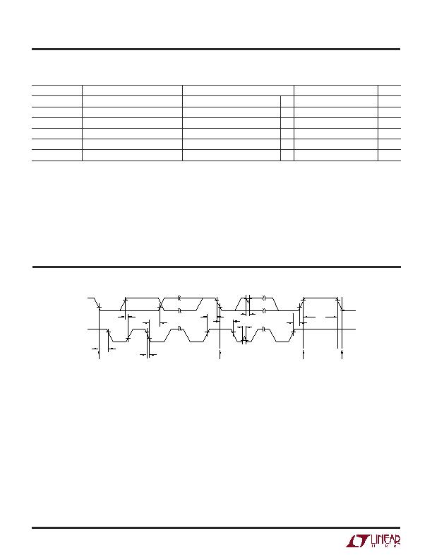
TI I G DIAGRA U
W
t
SU, DAT
t
SU, STO
t
SU, STA
t
BUF
t
HD, STA
t
SP
t
SP
t
HD, DATO,
t
HD, DATI
t
HD, STA
t
of
START
CONDITION
STOP
CONDITION
REPEATED START
CONDITION
START
CONDITION
SDA
SCL
4245 TDO1
ELECTRICAL CHARACTERISTICS
相关PDF资料 |
PDF描述 |
|---|---|
| 190-009-163R001 | CONN DB9 MALE R/A SOLDER SMD |
| ESA43DRMN | CONN EDGECARD 86POS .125 SQ WW |
| ISPLSI 2128E-135LT176 | IC PLD ISP 128I/O 7.5NS 176TQFP |
| EMA43DRMN | CONN EDGECARD 86POS .125 SQ WW |
| MIC39150-2.5BT | IC REG LDO 2.5V 1.5A TO-220 |
相关代理商/技术参数 |
参数描述 |
|---|---|
| AD7606BSTZ | 制造商:Analog Devices 功能描述:IC ADC 16BIT 200KSPS QFP-64 制造商:Analog Devices 功能描述:IC, ADC, 16BIT, 200KSPS, QFP-64 |
| AD7606BSTZ-4 | 功能描述:IC DAS W/ADC 16BIT 4CH 64LQFP RoHS:是 类别:集成电路 (IC) >> 数据采集 - ADCs/DAC - 专用型 系列:- 产品培训模块:Data Converter Basics 标准包装:1 系列:- 类型:电机控制 分辨率(位):12 b 采样率(每秒):1M 数据接口:串行,并联 电压电源:单电源 电源电压:2.7 V ~ 3.6 V,4.5 V ~ 5.5 V 工作温度:-40°C ~ 85°C 安装类型:表面贴装 封装/外壳:100-TQFP 供应商设备封装:100-TQFP(14x14) 包装:剪切带 (CT) 其它名称:296-18373-1 |
| AD7606BSTZ-4 | 制造商:Analog Devices 功能描述:IC, ADC, 16BIT, 200KSPS, QFP-64 |
| AD7606BSTZ-4RL | 功能描述:IC DAS W/ADC 16BIT 64LQFP RoHS:是 类别:集成电路 (IC) >> 数据采集 - ADCs/DAC - 专用型 系列:- 产品培训模块:Lead (SnPb) Finish for COTS Obsolescence Mitigation Program 标准包装:50 系列:- 类型:数据采集系统(DAS) 分辨率(位):16 b 采样率(每秒):21.94k 数据接口:MICROWIRE?,QSPI?,串行,SPI? 电压电源:模拟和数字 电源电压:1.8 V ~ 3.6 V 工作温度:-40°C ~ 85°C 安装类型:表面贴装 封装/外壳:40-WFQFN 裸露焊盘 供应商设备封装:40-TQFN-EP(6x6) 包装:托盘 |
| AD7606BSTZ-6 | 功能描述:IC DAS W/ADC 16BIT 6CH 64LQFP RoHS:是 类别:集成电路 (IC) >> 数据采集 - ADCs/DAC - 专用型 系列:- 产品培训模块:Lead (SnPb) Finish for COTS Obsolescence Mitigation Program 标准包装:50 系列:- 类型:数据采集系统(DAS) 分辨率(位):16 b 采样率(每秒):21.94k 数据接口:MICROWIRE?,QSPI?,串行,SPI? 电压电源:模拟和数字 电源电压:1.8 V ~ 3.6 V 工作温度:-40°C ~ 85°C 安装类型:表面贴装 封装/外壳:40-WFQFN 裸露焊盘 供应商设备封装:40-TQFN-EP(6x6) 包装:托盘 |
发布紧急采购,3分钟左右您将得到回复。