参数资料
| 型号: | AD7607BSTZ |
| 厂商: | Analog Devices Inc |
| 文件页数: | 22/32页 |
| 文件大小: | 0K |
| 描述: | IC DAS W/ADC 14BIT 8CH 64LQFP |
| 标准包装: | 1 |
| 类型: | 数据采集系统(DAS),ADC |
| 分辨率(位): | 14 b |
| 采样率(每秒): | 200k |
| 数据接口: | DSP,MICROWIRE?,并联,QSPI?,串行,SPI? |
| 电压电源: | 模拟和数字 |
| 电源电压: | 2.3 V ~ 5.25 V,4.75 V ~ 5.25 V |
| 工作温度: | -40°C ~ 85°C |
| 安装类型: | 表面贴装 |
| 封装/外壳: | 64-LQFP |
| 供应商设备封装: | 64-LQFP(10x10) |
| 包装: | 托盘 |
第1页第2页第3页第4页第5页第6页第7页第8页第9页第10页第11页第12页第13页第14页第15页第16页第17页第18页第19页第20页第21页当前第22页第23页第24页第25页第26页第27页第28页第29页第30页第31页第32页
Data Sheet
AD7607
Rev. B | Page 29 of 32
LAYOUT GUIDELINES
The printed circuit board that houses the AD7607 should be
designed so that the analog and digital sections are separated
and confined to different areas of the board.
At least one ground plane should be used. It can be common or
split between the digital and analog sections. In the case of the
split plane, the digital and analog ground planes should be joined
in only one place, preferably as close as possible to the AD7607.
If the AD7607 is in a system where multiple devices require
analog-to-digital ground connections, the connection should
still be made at only one point: a star ground point that should be
established as close as possible to the AD7607. Good connections
should be made to the ground plane. Avoid sharing one connection
for multiple ground pins. Use individual vias or multiple vias to
the ground plane for each ground pin.
Avoid running digital lines under the devices because doing so
couples noise onto the die. The analog ground plane should be
allowed to run under the AD7607 to avoid noise coupling. Fast
switching signals like CONVST A, CONVST B, or clocks should
be shielded with digital ground to avoid radiating noise to other
sections of the board, and they should never run near analog
signal paths. Avoid crossover of digital and analog signals. Traces
on layers in close proximity on the board should run at right angles
to each other to reduce the effect of feedthrough through the board.
The power supply lines to the AVCC and VDRIVE pins should use
as large a trace as possible to provide low impedance paths and
reduce the effect of glitches on the power supply lines. Where
possible, use supply planes and make good connections between
the AD7607 supply pins and the power tracks on the board.
Use a single via or multiple vias for each supply pin.
Good decoupling is also important in lowering the supply
impedance presented to the AD7607 and in reducing the
magnitude of the supply spikes. The decoupling capacitors should
be placed close to (ideally, right up against) these pins and their
corresponding ground pins. Place the decoupling capacitors for
the REFIN/REFOUT pin and the REFCAPA and REFCAPB
pins as close as possible to their respective AD7607 pins; and,
where possible, they should be placed on the same side of the
board as the AD7607 device.
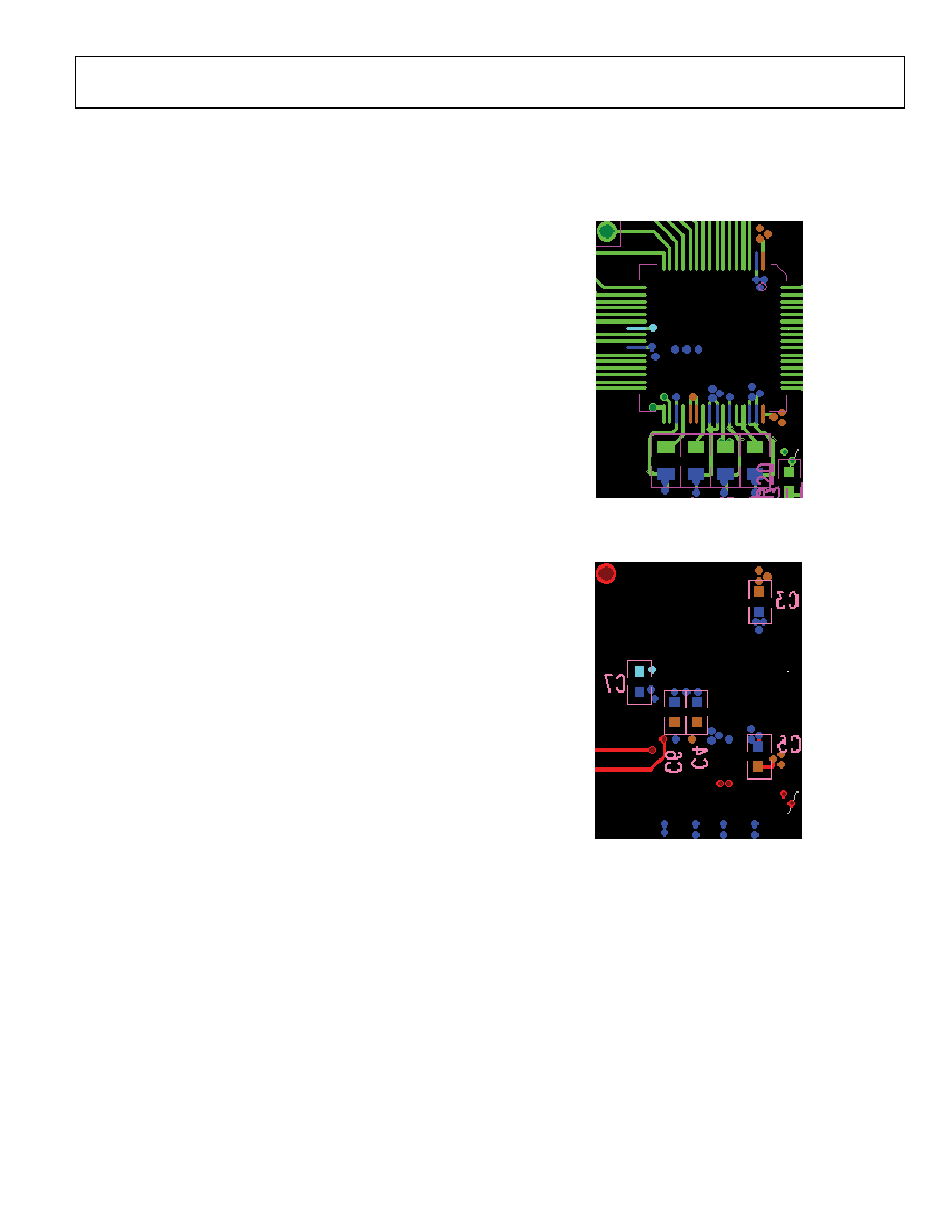
Figure 52 shows the recommended decoupling on the top layer
of the AD7607 board. Figure 53 shows bottom layer decoupling,
which is used for the four AVCC pins and the VDRIVE pin.
08096-
048
Figure 52. Top Layer Decoupling REFIN/REFOUT,
REFCAPA, REFCAPB, and REGCAP Pins
08096-
049
Figure 53. Bottom Layer Decoupling
相关PDF资料 |
PDF描述 |
|---|---|
| V110A5M200BG3 | CONVERTER MOD DC/DC 5V 200W |
| VI-24N-MY-S | CONVERTER MOD DC/DC 18.5V 50W |
| GTC020R-40-53S | CONN RCPT 60POS BOX MNT W/SCKT |
| GTC02R-40-62S | CONN RCPT 60POS BOX MNT W/SCKT |
| VI-24M-MY-S | CONVERTER MOD DC/DC 10V 50W |
相关代理商/技术参数 |
参数描述 |
|---|---|
| AD7607BSTZ-RL | 功能描述:IC DAS W/ADC 14BIT 8CH 64LQFP RoHS:是 类别:集成电路 (IC) >> 数据采集 - ADCs/DAC - 专用型 系列:- 产品培训模块:Lead (SnPb) Finish for COTS Obsolescence Mitigation Program 标准包装:50 系列:- 类型:数据采集系统(DAS) 分辨率(位):16 b 采样率(每秒):21.94k 数据接口:MICROWIRE?,QSPI?,串行,SPI? 电压电源:模拟和数字 电源电压:1.8 V ~ 3.6 V 工作温度:-40°C ~ 85°C 安装类型:表面贴装 封装/外壳:40-WFQFN 裸露焊盘 供应商设备封装:40-TQFN-EP(6x6) 包装:托盘 |
| AD7608 | 制造商:AD 制造商全称:Analog Devices 功能描述:8-Channel Differential DAS with 18-Bit |
| AD7608BSTZ | 功能描述:IC DAS W/ADC 18BIT 8CH 64LQFP RoHS:是 类别:集成电路 (IC) >> 数据采集 - ADCs/DAC - 专用型 系列:- 产品培训模块:Data Converter Basics 标准包装:1 系列:- 类型:电机控制 分辨率(位):12 b 采样率(每秒):1M 数据接口:串行,并联 电压电源:单电源 电源电压:2.7 V ~ 3.6 V,4.5 V ~ 5.5 V 工作温度:-40°C ~ 85°C 安装类型:表面贴装 封装/外壳:100-TQFP 供应商设备封装:100-TQFP(14x14) 包装:剪切带 (CT) 其它名称:296-18373-1 |
| AD7608BSTZ-RL | 功能描述:IC DAS W/ADC 18BIT 8CH 64LQFP RoHS:是 类别:集成电路 (IC) >> 数据采集 - ADCs/DAC - 专用型 系列:- 产品培训模块:Lead (SnPb) Finish for COTS Obsolescence Mitigation Program 标准包装:50 系列:- 类型:数据采集系统(DAS) 分辨率(位):16 b 采样率(每秒):21.94k 数据接口:MICROWIRE?,QSPI?,串行,SPI? 电压电源:模拟和数字 电源电压:1.8 V ~ 3.6 V 工作温度:-40°C ~ 85°C 安装类型:表面贴装 封装/外壳:40-WFQFN 裸露焊盘 供应商设备封装:40-TQFN-EP(6x6) 包装:托盘 |
| AD7609 | 制造商:AD 制造商全称:Analog Devices 功能描述:8-Channel Differential DAS with 18-Bit |
发布紧急采购,3分钟左右您将得到回复。