- 您现在的位置:买卖IC网 > PDF目录10521 > AD7612BCPZ (Analog Devices Inc)IC ADC 16BIT 750KSPS SAR 48LFCSP PDF资料下载
参数资料
| 型号: | AD7612BCPZ |
| 厂商: | Analog Devices Inc |
| 文件页数: | 10/32页 |
| 文件大小: | 0K |
| 描述: | IC ADC 16BIT 750KSPS SAR 48LFCSP |
| 标准包装: | 1 |
| 系列: | PulSAR® |
| 位数: | 16 |
| 采样率(每秒): | 750k |
| 数据接口: | 串行,并联 |
| 转换器数目: | 1 |
| 功率耗散(最大): | 230mW |
| 电压电源: | 模拟和数字 |
| 工作温度: | -40°C ~ 85°C |
| 安装类型: | 表面贴装 |
| 封装/外壳: | 48-VFQFN 裸露焊盘,CSP |
| 供应商设备封装: | 48-LFCSP-VQ(7x7) |
| 包装: | 托盘 |
| 输入数目和类型: | 1 个差分,双极 |
| 配用: | EVAL-AD7612CBZ-ND - BOARD EVALUATION FOR AD7612 |
第1页第2页第3页第4页第5页第6页第7页第8页第9页当前第10页第11页第12页第13页第14页第15页第16页第17页第18页第19页第20页第21页第22页第23页第24页第25页第26页第27页第28页第29页第30页第31页第32页
AD7612
Data Sheet
Rev. A | Page 18 of 32
MODES OF OPERATION
The AD7612 features three modes of operation: warp, normal,
and impulse. Each of these modes is more suitable to specific
applications. The mode is configured with the input pins, WARP
and IMPULSE, or via the configuration register. See Table 6 for
the pin details and the Hardware Configuration section and
Software Configuration section for programming the mode
selection with either pins or configuration register. Note that
when using the configuration register, the WARP and IMPULSE
inputs are don’t cares and should be tied to either high or low.
Warp Mode
Setting WARP = high and IMPULSE = low allow the fastest con-
version rate up to 750 kSPS. However, in this mode, the full
specified accuracy is guaranteed only when the time between
conversions does not exceed 1 ms. If the time between two
consecutive conversions is longer than 1 ms (after power-up),
the first conversion result should be ignored since in warp mode,
the ADC performs a background calibration during the SAR
conversion process. This calibration can drift if the time between
conversions exceeds 1 ms thus causing the first conversion to
appear offset. This mode makes the AD7612 ideal for applications
where both high accuracy and fast sample rate are required. In
addition, the AD7612 can run up to 900 kSPS throughput with
some performance degradation, mainly dc linearity.
Normal Mode
Setting WARP = IMPULSE = low or WARP = IMPULSE = high
allows the fastest mode (600 kSPS) without any limitation on
time between conversions. This mode makes the AD7612 ideal
for asynchronous applications such as data acquisition systems,
where both high accuracy and fast sample rate are required.
Impulse Mode
Setting WARP = low and IMPULSE = high uses the lowest power
dissipation mode and allows power saving between conversions.
The maximum throughput in this mode is 500 kSPS and in this
mode, the ADC powers down circuits after conversion making
the AD7612 ideal for battery-powered applications.
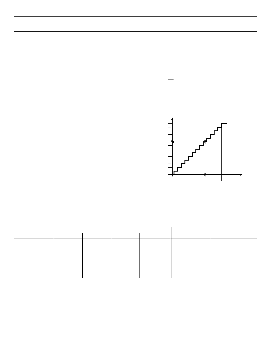
TRANSFER FUNCTIONS
Using the OB/2C digital input or via the configuration register,
the AD7612 offers two output codings: straight binary and twos
acteristic and digital output codes for the different analog input
ranges, VIN. Note that when using the configuration register, the
OB/2C input is a don’t care and should be tied to either high or low.
000...000
000...001
000...010
111...101
111...110
111...111
A
DC
CO
DE
(
S
tr
ai
g
h
tBi
n
ar
y)
ANALOG INPUT
+FSR – 1.5 LSB
+FSR –1LSB
–FSR + 1 LSB
–FSR
–FSR + 0.5 LSB
06
26
5-
0
26
Figure 26. ADC Ideal Transfer Function
Table 7. Output Codes and Ideal Input Voltages
VREF = 5 V
Digital Output Code
Description
VIN = 5 V
VIN = 10 V
VIN = ±5 V
VIN = ±10 V
Straight Binary
Twos Complement
FSR 1 LSB
4.999924 V
9.999847 V
+4.999847 V
+9.999695 V
0xFFFF1
0x7FFF1
FSR 2 LSB
4.999847 V
9.999695 V
+4.999695 V
+9.999390 V
0xFFFE
0x7FFE
Midscale + 1 LSB
2.500076 V
5.000153 V
+152.6 μV
+305.2 μV
0x8001
0x0001
Midscale
2.5 V
5.000000 V
0 V
0x8000
0x0000
Midscale 1 LSB
2.499924 V
4.999847 V
152.6 μV
305.2 μV
0x7FFF
0xFFFF
FSR + 1 LSB
76.3 μV
152.6 μV
4.999847 V
9.999695 V
0x0001
0x8001
FSR
0 V
5 V
10 V
0x00002
0x80002
1 This is also the code for overrange analog input (VIN+ VIN above VREF VREFGND).
2 This is also the code for overrange analog input (VIN+ VIN below VREF VREFGND).
相关PDF资料 |
PDF描述 |
|---|---|
| PT02E-22-55P | CONN RCPT 55 POS BOX MNT W/PINS |
| MS3102R28-5P | CONN RCPT 5POS BOX MNT W/PINS |
| MS3102E28-5P | CONN RCPT 5POS BOX MNT W/PINS |
| AD7612BSTZ | IC ADC 16BIT 750KSPS SAR 48-LQFP |
| AD7641BCPZ | IC ADC 18BIT 2MSPS SAR 48-LFCSP |
相关代理商/技术参数 |
参数描述 |
|---|---|
| AD7612BCPZ-RL | 功能描述:IC ADC 16BIT 750KSPS SAR 48LFCSP RoHS:是 类别:集成电路 (IC) >> 数据采集 - 模数转换器 系列:PulSAR® 标准包装:1 系列:- 位数:14 采样率(每秒):83k 数据接口:串行,并联 转换器数目:1 功率耗散(最大):95mW 电压电源:双 ± 工作温度:0°C ~ 70°C 安装类型:通孔 封装/外壳:28-DIP(0.600",15.24mm) 供应商设备封装:28-PDIP 包装:管件 输入数目和类型:1 个单端,双极 |
| AD7612BST | 制造商:Analog Devices 功能描述:ADC 16BIT 750KSPS SAR 48-LQFP 制造商:Analog Devices 功能描述:ADC, 16BIT, 750KSPS, SAR, 48-LQFP |
| AD7612BSTZ | 功能描述:IC ADC 16BIT 750KSPS SAR 48-LQFP RoHS:是 类别:集成电路 (IC) >> 数据采集 - 模数转换器 系列:PulSAR® 其它有关文件:TSA1204 View All Specifications 标准包装:1 系列:- 位数:12 采样率(每秒):20M 数据接口:并联 转换器数目:2 功率耗散(最大):155mW 电压电源:模拟和数字 工作温度:-40°C ~ 85°C 安装类型:表面贴装 封装/外壳:48-TQFP 供应商设备封装:48-TQFP(7x7) 包装:Digi-Reel® 输入数目和类型:4 个单端,单极;2 个差分,单极 产品目录页面:1156 (CN2011-ZH PDF) 其它名称:497-5435-6 |
| AD7612BSTZ-RL | 功能描述:IC ADC 16BIT 750KSPS SAR 48-LQFP RoHS:是 类别:集成电路 (IC) >> 数据采集 - 模数转换器 系列:PulSAR® 标准包装:1 系列:- 位数:14 采样率(每秒):83k 数据接口:串行,并联 转换器数目:1 功率耗散(最大):95mW 电压电源:双 ± 工作温度:0°C ~ 70°C 安装类型:通孔 封装/外壳:28-DIP(0.600",15.24mm) 供应商设备封装:28-PDIP 包装:管件 输入数目和类型:1 个单端,双极 |
| AD7616BSTZ | 功能描述:16 Bit Analog to Digital Converter 16 Input 2 SAR 80-LQFP (14x14) 制造商:analog devices inc. 系列:- 包装:托盘 零件状态:在售 位数:16 采样率(每秒):1M 输入数:16 输入类型:差分 数据接口:SPI,并联,DSP 配置:MUX-S/H-ADC 无线电 - S/H:ADC:1:1 A/D 转换器数:2 架构:SAR 参考类型:外部, 内部 电压 - 电源,模拟:5V 电压 - 电源,数字:2.3 V ~ 3.6 V 特性:同步采样 工作温度:-40°C ~ 125°C 封装/外壳:80-LQFP 供应商器件封装:80-LQFP(14x14) 标准包装:1 |
发布紧急采购,3分钟左右您将得到回复。