- 您现在的位置:买卖IC网 > PDF目录1982 > AD7688BCPZRL7 (Analog Devices Inc)IC ADC 16BIT SAR 500KSPS 10LFCSP PDF资料下载
参数资料
| 型号: | AD7688BCPZRL7 |
| 厂商: | Analog Devices Inc |
| 文件页数: | 14/28页 |
| 文件大小: | 0K |
| 描述: | IC ADC 16BIT SAR 500KSPS 10LFCSP |
| 标准包装: | 1 |
| 系列: | PulSAR® |
| 位数: | 16 |
| 采样率(每秒): | 500k |
| 数据接口: | DSP,MICROWIRE?,QSPI?,串行,SPI? |
| 转换器数目: | 1 |
| 功率耗散(最大): | 21.5mW |
| 电压电源: | 模拟和数字 |
| 工作温度: | -40°C ~ 85°C |
| 安装类型: | 表面贴装 |
| 封装/外壳: | 10-WFDFN 裸露焊盘,CSP |
| 供应商设备封装: | 10-LFCSP-WD(3x3) |
| 包装: | 标准包装 |
| 输入数目和类型: | 2 个单端,单极;2 个单端,双极;1 个差分,单极;1 个差分,双极 |
| 其它名称: | AD7688BCPZRL7DKR |
第1页第2页第3页第4页第5页第6页第7页第8页第9页第10页第11页第12页第13页当前第14页第15页第16页第17页第18页第19页第20页第21页第22页第23页第24页第25页第26页第27页第28页
AD7688
Rev. A | Page 21 of 28
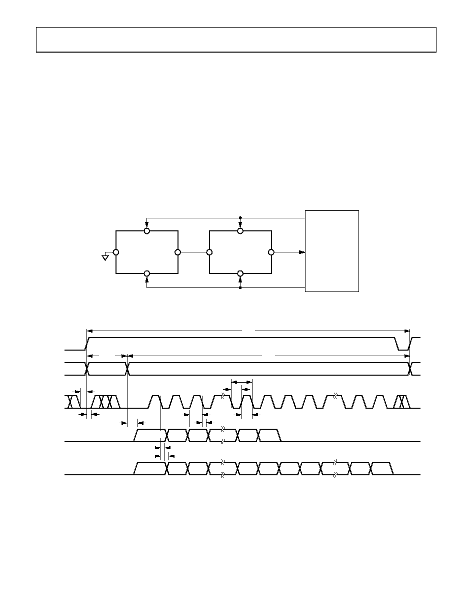
CHAIN MODE, NO BUSY INDICATOR
This mode can be used to daisy-chain multiple AD7688s on a 3-
wire serial interface. This feature is useful for reducing
component count and wiring connections, for example, in
isolated multiconverter applications or for systems with a
limited interfacing capacity. Data readback is analogous to
clocking a shift register.
A connection diagram example using two AD7688s is shown in
When SDI and CNV are low, SDO is driven low. With SCK low,
a rising edge on CNV initiates a conversion, selects the chain
mode, and disables the BUSY indicator. In this mode, CNV is
held high during the conversion phase and the subsequent data
readback. When the conversion is complete, the MSB is output
onto SDO and the AD7688 enters the acquisition phase and
powers down. The remaining data bits stored in the internal
shift register are then clocked by subsequent SCK falling edges.
For each ADC, SDI feeds the input of the internal shift register
and is clocked by the SCK falling edge. Each ADC in the chain
outputs its data MSB first, and 16 × N clocks are required to
readback the N ADCs. The data is valid on both SCK edges.
Although the rising edge can be used to capture the data, a
digital host using the SCK falling edge allows a faster reading
rate and, consequently more AD7688s in the chain, provided
the digital host has an acceptable hold time. The maximum
conversion rate may be reduced due to the total readback time.
For instance, with a 3 ns digital host set-up time and 3 V
interface, up to four AD7688s running at a conversion rate of
360 kSPS can be daisy-chained on a 3-wire port.
CLK
CONVERT
DATA IN
DIGITAL HOST
02973-
041
CNV
SCK
SDO
SDI
AD7688
B
CNV
SCK
SDO
SDI
AD7688
A
Figure 42. Chain Mode, No BUSY Indicator Connection Diagram
SDOA = SDIB
DA15
DA14
DA13
SCK
1
2
3
30
31
32
tSSDISCK
tHSDISC
tEN
CONVERSION
ACQUISITION
tCONV
tCYC
tACQ
ACQUISITION
CNV
DA1
14
15
tSCK
tSCKL
tSCKH
DA0
17
18
16
SDIA = 0
SDOB
DB15
DB14
DB13
DA1
DB1DB0DA15
DA14
tHSDO
tDSDO
tSSCKCNV
tHSCKCNV
DA0
02973-
042
Figure 43. Chain Mode, No BUSY Indicator Serial Interface Timing
相关PDF资料 |
PDF描述 |
|---|---|
| AD7689BCPZRL7 | IC ADC 16BIT 250KSPS 8CH 20LFCSP |
| AD7690BCPZRL | IC ADC 18BIT 400KSPS 10-LFCSP |
| AD7691BCPZRL7 | IC ADC 18BIT SAR 250KSPS 10LFCSP |
| AD7693BRMZRL7 | IC ADC 16BIT 500KSPS 10-MSOP |
| AD7694ARMZ | IC ADC 16BIT SAR 250KSPS 8MSOP |
相关代理商/技术参数 |
参数描述 |
|---|---|
| AD7688BRM | 制造商:Analog Devices 功能描述:ADC Single SAR 500ksps 16-bit Serial 10-Pin MSOP Tube 制造商:Rochester Electronics LLC 功能描述:16-BIT DIFF, 550KSPS SERIAL MSOP ADC - Bulk 制造商:Analog Devices 功能描述:IC 16-BIT ADC |
| AD7688BRMRL7 | 制造商:Analog Devices 功能描述:ADC Single SAR 500ksps 16-bit Serial 10-Pin MSOP T/R |
| AD7688BRMZ | 功能描述:IC ADC DIFF 16BIT 500KSPS 10MSOP RoHS:是 类别:集成电路 (IC) >> 数据采集 - 模数转换器 系列:PulSAR® 标准包装:1 系列:microPOWER™ 位数:8 采样率(每秒):1M 数据接口:串行,SPI? 转换器数目:1 功率耗散(最大):- 电压电源:模拟和数字 工作温度:-40°C ~ 125°C 安装类型:表面贴装 封装/外壳:24-VFQFN 裸露焊盘 供应商设备封装:24-VQFN 裸露焊盘(4x4) 包装:Digi-Reel® 输入数目和类型:8 个单端,单极 产品目录页面:892 (CN2011-ZH PDF) 其它名称:296-25851-6 |
| AD7688BRMZRL7 | 功能描述:IC ADC 16BIT 500KSPS 10MSOP RoHS:是 类别:集成电路 (IC) >> 数据采集 - 模数转换器 系列:PulSAR® 标准包装:1,000 系列:- 位数:12 采样率(每秒):300k 数据接口:并联 转换器数目:1 功率耗散(最大):75mW 电压电源:单电源 工作温度:0°C ~ 70°C 安装类型:表面贴装 封装/外壳:24-SOIC(0.295",7.50mm 宽) 供应商设备封装:24-SOIC 包装:带卷 (TR) 输入数目和类型:1 个单端,单极;1 个单端,双极 |
| AD7689 | 制造商:AD 制造商全称:Analog Devices 功能描述:14-Bit, 8-Channel, 250 kSPS PulSAR ADC |
发布紧急采购,3分钟左右您将得到回复。