- 您现在的位置:买卖IC网 > PDF目录10674 > AD7689ACPZ (Analog Devices Inc)IC ADC 16BIT 250KSPS 8CH 20LFCSP PDF资料下载
参数资料
| 型号: | AD7689ACPZ |
| 厂商: | Analog Devices Inc |
| 文件页数: | 13/32页 |
| 文件大小: | 0K |
| 描述: | IC ADC 16BIT 250KSPS 8CH 20LFCSP |
| 产品培训模块: | Power Line Monitoring Motor Control |
| 产品变化通告: | Startup Circuitry Design Improvement Change 15/April/2009 |
| 标准包装: | 1 |
| 系列: | PulSAR® |
| 位数: | 16 |
| 采样率(每秒): | 250k |
| 数据接口: | DSP,MICROWIRE?,QSPI?,串行,SPI? |
| 转换器数目: | 1 |
| 功率耗散(最大): | 21mW |
| 电压电源: | 模拟和数字 |
| 工作温度: | -40°C ~ 85°C |
| 安装类型: | 表面贴装 |
| 封装/外壳: | 20-VFQFN 裸露焊盘,CSP |
| 供应商设备封装: | 20-LFCSP-VQ |
| 包装: | 管件 |
| 输入数目和类型: | 8 个单端,单极;4 个差分,双极;4 个伪差分,双极 |
| 产品目录页面: | 778 (CN2011-ZH PDF) |
第1页第2页第3页第4页第5页第6页第7页第8页第9页第10页第11页第12页当前第13页第14页第15页第16页第17页第18页第19页第20页第21页第22页第23页第24页第25页第26页第27页第28页第29页第30页第31页第32页
AD7682/AD7689
Data Sheet
Rev. D | Page 20 of 32
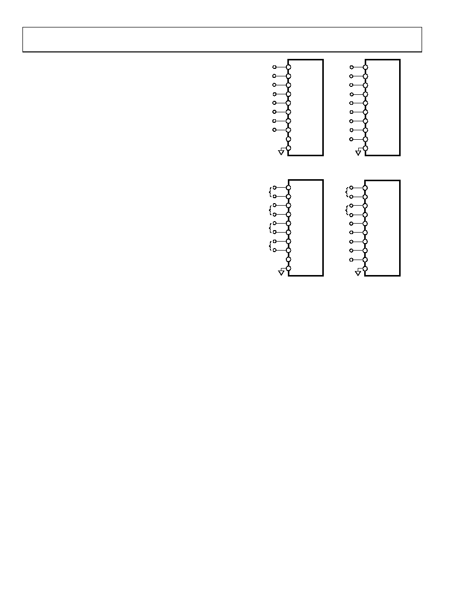
Input Configurations
Figure 30 shows the different methods for configuring the analog
inputs with the configuration register, CFG[12:10]. Refer to the
Configuration Register, CFG, section for more details.
The analog inputs can be configured as
Figure 30A, single-ended referenced to system ground;
CFG[12:10] = 1112.
In this configuration, all inputs (IN[7:0]) have a range of
GND to VREF.
Figure 30B, bipolar differential with a common reference
point; COM = VREF/2; CFG[12:10] = 0102.
Unipolar differential with COM connected to a ground
sense; CFG[12:10] = 1102.
In this configuration, all inputs IN[7:0] have a range of
GND to VREF.
Figure 30C, bipolar differential pairs with the negative
input channel referenced to VREF/2; CFG[12:10] = 00X2.
Unipolar differential pairs with the negative input channel
referenced to a ground sense; CFG[12:10] = 10X2.
In these configurations, the positive input channels have
the range of GND to VREF. The negative input channels are
a sense referred to VREF/2 for bipolar pairs, or GND for
unipolar pairs. The positive channel is configured with
CFG[9:7]. If CFG[9:7] is even, then IN0, IN2, IN4, and IN6
are used. If CFG[9:7] is odd, then IN1, IN3, IN5, and IN7
are used, as indicated by the channels with parentheses in
Figure 30C. For example, for IN0/IN1 pairs with the
positive channel on IN0, CFG[9:7] = 0002. For IN4/IN5
pairs with the positive channel on IN5, CFG[9:7] = 1012.
Note that for the sequencer, detailed in the Channel
Sequencer section, the positive channels are always IN0,
IN2, IN4, and IN6.
Figure 30D, inputs configured in any of the preceding
combinations (showing that the AD7682/AD7689 can be
configured dynamically).
GND
COM
CH0+
CH3+
CH1+
CH2+
CH4+
CH5+
CH6+
CH7+
CH0+
CH3+
CH1+
CH2+
CH4+
CH5+
CH6+
CH7+
COM–
GND
COM
IN1
IN0
IN2
IN3
IN4
IN5
IN6
IN7
IN1
IN0
IN2
IN3
IN4
IN5
IN6
IN7
IN1
IN0
IN2
IN3
IN4
IN5
IN6
IN7
IN1
IN0
IN2
IN3
IN4
IN5
IN6
IN7
A—8 CHANNELS,
SINGLE ENDED
B—8 CHANNELS,
COMMON REFERNCE
GND
COM
CH0+ (–)
CH1+ (–)
CH2+ (–)
CH3+ (–)
CH0– (+)
CH1– (+)
CH0+ (–)
CH1+ (–)
CH0– (+)
CH1– (+)
CH2– (+)
CH3– (+)
C—4 CHANNELS,
DIFFERENTIAL
GND
COM
CH2+
CH3+
CH4+
CH5+
D—COMBINATION
COM–
07
35
3-
03
2
Figure 30. Multiplexed Analog Input Configurations
Sequencer
scanning channels in a repeated fashion. Refer to the Channel
Sequencer section for further details of the sequencer operation.
Source Resistance
When the source impedance of the driving circuit is low, the
ances significantly affect the ac performance, especially THD.
The dc performances are less sensitive to the input impedance.
The maximum source impedance depends on the amount of
THD that can be tolerated. The THD degrades as a function of
the source impedance and the maximum input frequency.
相关PDF资料 |
PDF描述 |
|---|---|
| LTC1598CG#PBF | IC A/D CONV 12BIT SRL 8CH 24SSOP |
| KA339A | IC COMPARATOR QUAD 14-DIP |
| KA339 | IC COMPARATOR QUAD 14-DIP |
| AD7683ARMZ | IC ADC 16BIT 100KSPS 8-MSOP |
| VI-2T0-IX-B1 | CONVERTER MOD DC/DC 5V 75W |
相关代理商/技术参数 |
参数描述 |
|---|---|
| AD7689ACPZRL7 | 功能描述:IC ADC 16BIT 250KSPS 8CH 20LFCSP RoHS:是 类别:集成电路 (IC) >> 数据采集 - 模数转换器 系列:PulSAR® 标准包装:1,000 系列:- 位数:16 采样率(每秒):45k 数据接口:串行 转换器数目:2 功率耗散(最大):315mW 电压电源:模拟和数字 工作温度:0°C ~ 70°C 安装类型:表面贴装 封装/外壳:28-SOIC(0.295",7.50mm 宽) 供应商设备封装:28-SOIC W 包装:带卷 (TR) 输入数目和类型:2 个单端,单极 |
| AD7689BCBZ-RL7 | 功能描述:16 Bit Analog to Digital Converter 8 Input 1 SAR 20-WLCSP (2.39x2.39) 制造商:analog devices inc. 系列:- 包装:剪切带(CT) 零件状态:有效 位数:16 采样率(每秒):250k 输入数:8 输入类型:差分,个伪差分,单端 数据接口:SPI,DSP 配置:MUX-S/H-ADC 无线电 - S/H:ADC:1:1 A/D 转换器数:1 架构:SAR 参考类型:外部, 内部 电压 - 电源,模拟:2.3 V ~ 5.5 V 电压 - 电源,数字:1.8 V ~ 5.5 V 特性:温度传感器 工作温度:-40°C ~ 85°C 封装/外壳:20-UFBGA,WLCSP 供应商器件封装:20-WLCSP(2.39x2.39) 标准包装:1 |
| AD7689BCPZ | 功能描述:IC ADC 16BIT 250KSPS 8CH 20LFCSP RoHS:是 类别:集成电路 (IC) >> 数据采集 - 模数转换器 系列:PulSAR® 标准包装:1 系列:microPOWER™ 位数:8 采样率(每秒):1M 数据接口:串行,SPI? 转换器数目:1 功率耗散(最大):- 电压电源:模拟和数字 工作温度:-40°C ~ 125°C 安装类型:表面贴装 封装/外壳:24-VFQFN 裸露焊盘 供应商设备封装:24-VQFN 裸露焊盘(4x4) 包装:Digi-Reel® 输入数目和类型:8 个单端,单极 产品目录页面:892 (CN2011-ZH PDF) 其它名称:296-25851-6 |
| AD7689BCPZ | 制造商:Analog Devices 功能描述:IC ADC 16BIT 250KSPS LFCSP-20 |
| AD7689BCPZRL7 | 功能描述:IC ADC 16BIT 250KSPS 8CH 20LFCSP RoHS:是 类别:集成电路 (IC) >> 数据采集 - 模数转换器 系列:PulSAR® 标准包装:1,000 系列:- 位数:16 采样率(每秒):45k 数据接口:串行 转换器数目:2 功率耗散(最大):315mW 电压电源:模拟和数字 工作温度:0°C ~ 70°C 安装类型:表面贴装 封装/外壳:28-SOIC(0.295",7.50mm 宽) 供应商设备封装:28-SOIC W 包装:带卷 (TR) 输入数目和类型:2 个单端,单极 |
发布紧急采购,3分钟左右您将得到回复。