- 您现在的位置:买卖IC网 > PDF目录10658 > AD7690BRMZ (Analog Devices Inc)IC ADC 18BIT 400KSPS 10MSOP PDF资料下载
参数资料
| 型号: | AD7690BRMZ |
| 厂商: | Analog Devices Inc |
| 文件页数: | 16/24页 |
| 文件大小: | 0K |
| 描述: | IC ADC 18BIT 400KSPS 10MSOP |
| 标准包装: | 1 |
| 系列: | PulSAR® |
| 位数: | 18 |
| 采样率(每秒): | 400k |
| 数据接口: | DSP,MICROWIRE?,QSPI?,串行,SPI? |
| 转换器数目: | 1 |
| 功率耗散(最大): | 20mW |
| 电压电源: | 模拟和数字 |
| 工作温度: | -40°C ~ 85°C |
| 安装类型: | 表面贴装 |
| 封装/外壳: | 10-TFSOP,10-MSOP(0.118",3.00mm 宽) |
| 供应商设备封装: | 10-MSOP |
| 包装: | 管件 |
| 输入数目和类型: | 1 个差分,双极 |
| 产品目录页面: | 778 (CN2011-ZH PDF) |
AD7690
Rev. B | Page 23 of 24
APPLICATION HINTS
LAYOUT
The printed circuit board that houses the AD7690 should be
designed so that the analog and digital sections are separated
and confined to certain areas of the board. The pinout of the
AD7690, with its analog signals on the left side and its digital
signals on the right side, eases this task.
Avoid running digital lines under the device because these
couple noise onto the die unless a ground plane under the
AD7690 is used as a shield. Fast switching signals, such as CNV
or clocks, should not run near analog signal paths. Crossover of
digital and analog signals should be avoided.
At least one ground plane should be used. It can be common or
split between the digital and analog sections. In the latter case,
the planes should be joined underneath the AD7690s.
The AD7690 voltage reference input REF has a dynamic input
impedance and should be decoupled with minimal parasitic
inductances. This is done by placing the reference decoupling
ceramic capacitor close to, ideally right up against, the REF and
GND pins and connecting them with wide, low impedance traces.
Finally, the AD7690 VDD and VIO power supplies should be
decoupled with ceramic capacitors, typically 100 nF, placed
close to the AD7690 and connected using short, wide traces to
provide low impedance paths and to reduce the effect of glitches
on the power supply lines.
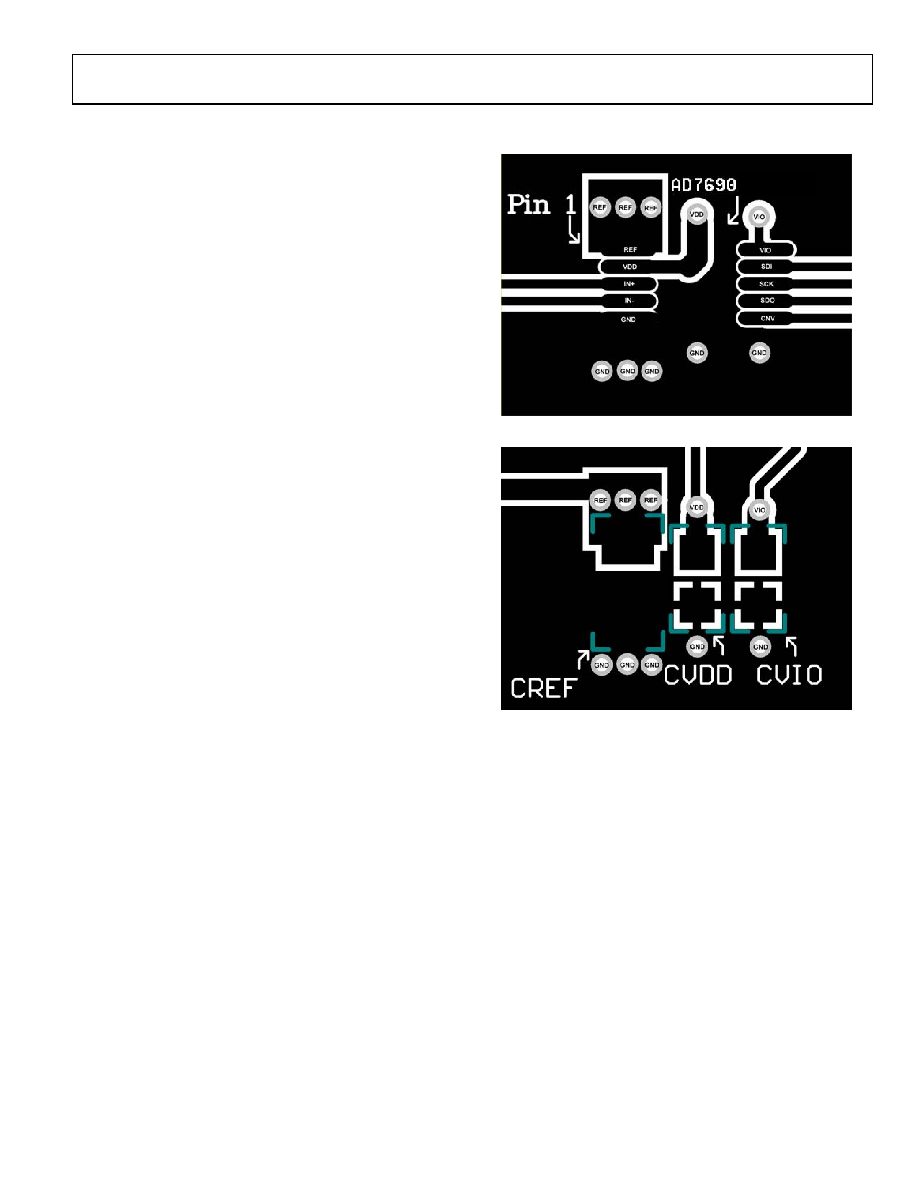
An example of a layout following these rules is shown in
Figure 46 and Figure 47.
EVALUATING THE AD7690’S PERFORMANCE
Other recommended layouts for the AD7690 are outlined
in the documentation of the evaluation board (EVAL-
AD7690CBZ). The evaluation board package includes
a fully assembled and tested evaluation board, documentation,
and software for controlling the board from a PC via the
0
57
92
-0
23
Figure 46. Example Layout of the AD7690 (Top Layer)
05
79
2-
0
24
Figure 47. Example Layout of the AD7690 (Bottom Layer)
相关PDF资料 |
PDF描述 |
|---|---|
| MAX933CSA+T | IC COMPARATOR W/REF 8-SOIC |
| VE-B1T-IV-F3 | CONVERTER MOD DC/DC 6.5V 150W |
| VE-B1T-IV-F2 | CONVERTER MOD DC/DC 6.5V 150W |
| MAX982CSA+T | IC COMPARATOR OD 8-SOIC |
| AD7710ARZ | IC ADC 24BIT DIFF INP 24-SOIC |
相关代理商/技术参数 |
参数描述 |
|---|---|
| AD7690BRMZ-RL7 | 功能描述:IC ADC 18BIT 400KSPS 10-MSOP RoHS:是 类别:集成电路 (IC) >> 数据采集 - 模数转换器 系列:PulSAR® 标准包装:1 系列:- 位数:14 采样率(每秒):83k 数据接口:串行,并联 转换器数目:1 功率耗散(最大):95mW 电压电源:双 ± 工作温度:0°C ~ 70°C 安装类型:通孔 封装/外壳:28-DIP(0.600",15.24mm) 供应商设备封装:28-PDIP 包装:管件 输入数目和类型:1 个单端,双极 |
| AD7690BRNZ | 制造商:Analog Devices 功能描述: |
| AD7691 | 制造商:AD 制造商全称:Analog Devices 功能描述:16-Bit Lower Power |
| AD76911 | 制造商:AD 制造商全称:Analog Devices 功能描述:18-Bit, 2 MSPS PulSAR 15 mW ADC in LFCSP (QFN) |
| AD7691BCPZ-R2 | 制造商:Rochester Electronics LLC 功能描述: 制造商:Analog Devices 功能描述: |
发布紧急采购,3分钟左右您将得到回复。