- 您现在的位置:买卖IC网 > PDF目录10556 > AD7693BCPZRL7 (Analog Devices Inc)IC ADC 16BIT 500KSPS 10-LFCSP PDF资料下载
参数资料
| 型号: | AD7693BCPZRL7 |
| 厂商: | Analog Devices Inc |
| 文件页数: | 22/24页 |
| 文件大小: | 0K |
| 描述: | IC ADC 16BIT 500KSPS 10-LFCSP |
| 标准包装: | 1 |
| 系列: | PulSAR® |
| 位数: | 16 |
| 采样率(每秒): | 500k |
| 数据接口: | DSP,MICROWIRE?,QSPI?,串行,SPI? |
| 转换器数目: | 1 |
| 功率耗散(最大): | 21.5mW |
| 电压电源: | 模拟和数字 |
| 工作温度: | -40°C ~ 85°C |
| 安装类型: | 表面贴装 |
| 封装/外壳: | 10-WFDFN 裸露焊盘,CSP |
| 供应商设备封装: | 10-LFCSP-WD(3x3) |
| 包装: | 标准包装 |
| 输入数目和类型: | 1 个差分,双极 |
| 其它名称: | AD7693BCPZRL7DKR |
AD7693
Rev. A | Page 7 of 24
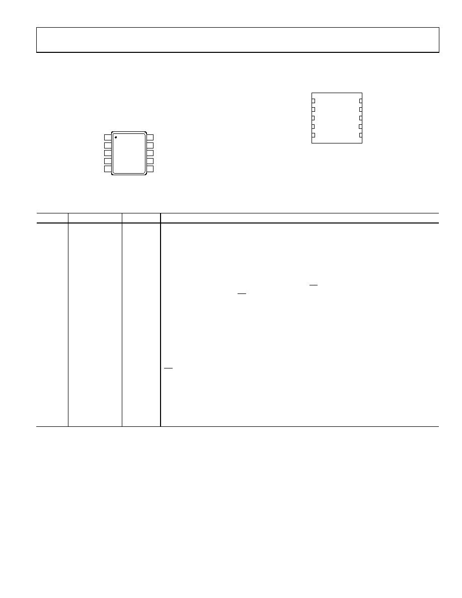
PIN CONFIGURATIONS AND FUNCTION DESCRIPTIONS
REF 1
VDD 2
IN+ 3
IN– 4
GND 5
VIO
10
SDI
9
SCK
8
SDO
7
CNV
6
AD7693
TOP VIEW
(Not to Scale)
06
39
4-
00
5
Figure 5. 10-Lead MSOP Pin Configuration
1
REF
2
VDD
3
IN+
4
IN–
5
GND
NOTES
1. THE EXPOSED PAD IS CONNECTED
TO GND. THIS CONNECTION IS NOT
REQUIRED TO MEET THE ELECTRICAL
PERFORMANCES.
10 VIO
9SDI
8SCK
7SDO
6CNV
TOP VIEW
(Not to Scale)
AD7693
05
793-
006
Figure 6. 10-Lead QFN (LFCSP) Pin Configuration
Table 6. Pin Function Descriptions
Pin No.
Mnemonic
Type1
Description
1
REF
AI
Reference Input Voltage. The REF range is from 0.5 V to VDD. It is referred to the GND pin. This
pin should be decoupled closely to the pin with a 10 μF capacitor.
2
VDD
P
Power Supply.
3
IN+
AI
Differential Positive Analog Input.
4
IN
AI
Differential Negative Analog Input.
5
GND
P
Power Supply Ground.
6
CNV
DI
Convert Input. This input has multiple functions. On its leading edge, it initiates the conversions
and selects the interface mode of the part: chain or CS mode. In chain mode, the data should be
read when CNV is high. In CS mode, the SDO pin is enabled when CNV is low.
7
SDO
DO
Serial Data Output. The conversion result is output on this pin. It is synchronized to SCK.
8
SCK
DI
Serial Data Clock Input. When the part is selected, the conversion result is shifted out by this
clock.
9
SDI
DI
Serial Data Input. This input provides multiple features. It selects the interface mode of the ADC
as follows:
Chain mode is selected if SDI is low during the CNV rising edge. In this mode, SDI is used as a
data input to daisy-chain the conversion results of two or more ADCs onto a single SDO line.
The digital data level on SDI is output on SDO with a delay of 16 SCK cycles.
CS mode is selected if SDI is high during the CNV rising edge. In this mode, either SDI or CNV
can enable the serial output signals when low and if SDI or CNV is low when the conversion is
complete, the busy indicator feature is enabled.
10
VIO
P
Input/Output Interface Digital Power. Nominally at the same supply as the host interface (1.8 V,
2.5 V, 3 V, or 5 V).
EPAD
Exposed Pad. The exposed pad is connected to GND. This connection is not required to meet
the electrical performances. The exposed pad is only on the 10-Lead QFN (LFCSP).
1AI = analog input, DI = digital input, DO = digital output, and P = power.
相关PDF资料 |
PDF描述 |
|---|---|
| VI-J5P-MW-F1 | CONVERTER MOD DC/DC 13.8V 100W |
| VI-J5M-MW-F4 | CONVERTER MOD DC/DC 10V 100W |
| TMK325B7106MM-T | CAP CER 10UF 25V 20% X7R 1210 |
| VI-J5M-MW-F3 | CONVERTER MOD DC/DC 10V 100W |
| VI-JV1-MY-F3 | CONVERTER MOD DC/DC 12V 50W |
相关代理商/技术参数 |
参数描述 |
|---|---|
| AD7693BRMZ | 功能描述:IC ADC 16BIT 500KSPS 10-MSOP RoHS:是 类别:集成电路 (IC) >> 数据采集 - 模数转换器 系列:PulSAR® 标准包装:1 系列:microPOWER™ 位数:8 采样率(每秒):1M 数据接口:串行,SPI? 转换器数目:1 功率耗散(最大):- 电压电源:模拟和数字 工作温度:-40°C ~ 125°C 安装类型:表面贴装 封装/外壳:24-VFQFN 裸露焊盘 供应商设备封装:24-VQFN 裸露焊盘(4x4) 包装:Digi-Reel® 输入数目和类型:8 个单端,单极 产品目录页面:892 (CN2011-ZH PDF) 其它名称:296-25851-6 |
| AD7693BRMZRL7 | 功能描述:IC ADC 16BIT 500KSPS 10-MSOP RoHS:是 类别:集成电路 (IC) >> 数据采集 - 模数转换器 系列:PulSAR® 标准包装:1 系列:- 位数:14 采样率(每秒):83k 数据接口:串行,并联 转换器数目:1 功率耗散(最大):95mW 电压电源:双 ± 工作温度:0°C ~ 70°C 安装类型:通孔 封装/外壳:28-DIP(0.600",15.24mm) 供应商设备封装:28-PDIP 包装:管件 输入数目和类型:1 个单端,双极 |
| AD7694 | 制造商:AD 制造商全称:Analog Devices 功能描述:16-Bit Lower Power |
| AD7694_05 | 制造商:AD 制造商全称:Analog Devices 功能描述:16-Bit, 250 kSPS PulSAR ADC in MSOP |
| AD7694ARM | 制造商:Rochester Electronics LLC 功能描述: 制造商:Analog Devices 功能描述: |
发布紧急采购,3分钟左右您将得到回复。