- 您现在的位置:买卖IC网 > PDF目录10311 > AD7705BRZ-REEL (Analog Devices Inc)IC ADC 16BIT 2CHAN 16SOIC PDF资料下载
参数资料
| 型号: | AD7705BRZ-REEL |
| 厂商: | Analog Devices Inc |
| 文件页数: | 2/44页 |
| 文件大小: | 0K |
| 描述: | IC ADC 16BIT 2CHAN 16SOIC |
| 标准包装: | 1,000 |
| 位数: | 16 |
| 采样率(每秒): | 500 |
| 数据接口: | DSP,MICROWIRE?,QSPI?,串行,SPI? |
| 转换器数目: | 1 |
| 功率耗散(最大): | 1mW |
| 电压电源: | 单电源 |
| 工作温度: | -40°C ~ 85°C |
| 安装类型: | 表面贴装 |
| 封装/外壳: | 16-SOIC(0.295",7.50mm 宽) |
| 供应商设备封装: | 16-SOIC W |
| 包装: | 带卷 (TR) |
| 输入数目和类型: | 2 个差分,单极;2 个差分,双极 |
| 配用: | EVAL-AD7705EBZ-ND - BOARD EVALUATION FOR AD7705 |
第1页当前第2页第3页第4页第5页第6页第7页第8页第9页第10页第11页第12页第13页第14页第15页第16页第17页第18页第19页第20页第21页第22页第23页第24页第25页第26页第27页第28页第29页第30页第31页第32页第33页第34页第35页第36页第37页第38页第39页第40页第41页第42页第43页第44页
AD7705/AD7706
Rev. C | Page 10 of 44
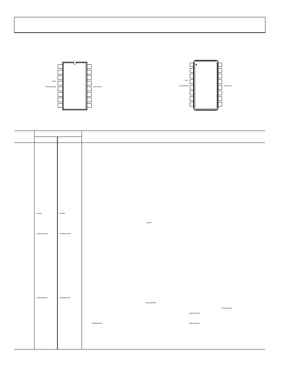
PIN CONFIGURATIONS AND FUNCTION DESCRIPTIONS
SCLK
1
MCLK IN
2
MCLK OUT
3
CS
4
GND
16
VDD
15
DIN
14
DOUT
13
RESET
5
DRDY
12
AIN2(+)
6
AIN2(–)
11
AIN1(+)
7
REF IN(–)
10
AIN1(–)
8
REF IN(+)
9
AD7705
TOP VIEW
(Not to Scale)
01166-003
Figure 3. AD7705 Pin Configuration
1
2
3
4
5
6
7
8
16
15
14
13
12
11
10
9
MCLK IN
MCLK OUT
CS
AIN2
AIN1
RESET
SCLK
VDD
DIN
DOUT
REF IN(–)
COMMON
REF IN(+)
AIN3
DRDY
GND
AD7706
TOP VIEW
(Not to Scale)
01166-004
Figure 4. AD7706 Pin Configuration
Table 4. Pin Function Descriptions
Mnemonic
Pin No.
AD7705
AD7706
Description
1
SCLK
Serial Clock. An external serial clock is applied to the Schmitt-triggered logic input to access serial
data from the AD7705/AD7706. This serial clock can be a continuous clock with all data transmitted in
a continuous train of pulses. Alternatively, it can be a noncontinuous clock with the information
transmitted to the AD7705/AD7706 in smaller batches of data.
2
MCLK IN
Master Clock Signal. This can be provided in the form of a crystal/resonator or external clock. A
crystal/resonator can be tied across the Pin MCLK IN and Pin MCLK OUT. Alternatively, the MCLK IN
pin can be driven with a CMOS-compatible clock with the MCLK OUT pin left unconnected. The parts
can be operated with clock frequencies in the range of 500 kHz to 5 MHz.
3
MCLK OUT
When the master clock for these devices is a crystal/resonator, the crystal/resonator is connected
between Pin MCLK IN and Pin MCLK OUT. If an external clock is applied to Pin MCLK IN, Pin MCLK OUT
provides an inverted clock signal. This clock can be used to provide a clock source for external
circuitry and is capable of driving 1 CMOS load. If the user does not require this clock externally, Pin
MCLK OUT can be turned off via the CLKDIS bit of the clock register. This ensures that the part does
not unnecessarily burn power driving capacitive loads on Pin MCLK OUT.
4
CS
Chip Select. Active low logic input used to select the AD7705/AD7706. With this input hardwired low,
the AD7705/AD7706 can operate in its 3-wire interface mode with Pin SCLK, Pin DIN, and Pin DOUT
used to interface to the device. The CS pin can be used to select the device communicating with the
AD7705/AD7706.
5
RESET
Logic Input. Active low input that resets the control logic, interface logic, calibration coefficients,
digital filter, and analog modulator of the parts to power-on status.
6
AIN2(+)
AIN1
Positive Input of the Differential Analog Input Pair AIN2(+)/AIN2() for AD7705. Channel 1 for AD7706.
7
AIN1(+)
AIN2
Positive Input of the Differential Analog Input Pair AIN1(+)/AIN1() for AD7705. Channel 2 for AD7706.
8
AIN1()
COMMON
Negative Input of the Differential Analog Input Pair AIN1(+)/AIN1() for AD7705. COMMON input for
AD7706 with Channel 1, Channel 2, and Channel 3 referenced to this input.
9
REF IN(+)
Reference Input. Positive input of the differential reference input to the AD7705/AD7706. The reference
input is differential with the provision that REF IN(+) must be greater than REF IN().
REF IN(+) can lie anywhere between VDD and GND.
10
REF IN()
Reference Input. Negative input of the differential reference input to the AD7705/AD7706. The
REF IN() can lie anywhere between VDD and GND, provided that REF IN(+) is greater than REF IN().
11
AIN2()
AIN3
Negative Input of the Differential Analog Input Pair AIN2(+)/AIN2() for AD7705. Channel 3 for AD7706.
12
DRDY
Logic Output. A logic low on this output indicates that a new output word is available from the
AD7705/AD7706 data register. The DRDY pin returns high upon completion of a read operation of a
full output word. If no data read has taken place between output updates, the DRDY line returns high
for 500 × tCLK IN cycles prior to the next output update. While DRDY is high, a read operation should
neither be attempted nor in progress to avoid reading from the data register as it is being updated.
The DRDY line returns low after the update has taken place. DRDY is also used to indicate when the
AD7705/AD7706 has completed its on-chip calibration sequence.
13
DOUT
Serial Data Output. Serial data is read from the output shift register on the part. The output shift
register can contain information from the setup register, communication register, clock register, or
data register, depending on the register selection bits of the communication register.
相关PDF资料 |
PDF描述 |
|---|---|
| CXS3102A14S1S | CONN RCPT 3POS PNL MNT SKT |
| VE-BN1-IX-B1 | CONVERTER MOD DC/DC 12V 75W |
| AD9609BCPZRL7-65 | IC ADC 10BIT SPI/SRL 65M 32LFCSP |
| VE-BN1-IW-B1 | CONVERTER MOD DC/DC 12V 100W |
| AD7940BRMZ-REEL7 | IC ADC 14BIT 100KSPS 8MSOP |
相关代理商/技术参数 |
参数描述 |
|---|---|
| AD7705BRZ-REEL1 | 制造商:AD 制造商全称:Analog Devices 功能描述:3 V/5 V, 1 mW, 2-/3-Channel, 16-Bit, Sigma-Delta ADCs |
| AD7705BRZ-REEL7 | 功能描述:IC ADC 16BIT 2CHAN 16SOIC RoHS:是 类别:集成电路 (IC) >> 数据采集 - 模数转换器 系列:- 标准包装:1,000 系列:- 位数:16 采样率(每秒):45k 数据接口:串行 转换器数目:2 功率耗散(最大):315mW 电压电源:模拟和数字 工作温度:0°C ~ 70°C 安装类型:表面贴装 封装/外壳:28-SOIC(0.295",7.50mm 宽) 供应商设备封装:28-SOIC W 包装:带卷 (TR) 输入数目和类型:2 个单端,单极 |
| AD7705BRZ-REEL71 | 制造商:AD 制造商全称:Analog Devices 功能描述:3 V/5 V, 1 mW, 2-/3-Channel, 16-Bit, Sigma-Delta ADCs |
| AD7705EB | 制造商:AD 制造商全称:Analog Devices 功能描述:3 V/5 V 1 mW 2-/3-Channel 16-Bit Sigma-Delta ADCs(264.12 k) |
| AD7706 | 制造商:AD 制造商全称:Analog Devices 功能描述:3 V/5 V, 1 mW 2-/3-Channel 16-Bit, Sigma-Delta ADCs |
发布紧急采购,3分钟左右您将得到回复。