- 您现在的位置:买卖IC网 > PDF目录10527 > AD7711ANZ (Analog Devices Inc)IC ADC 24BIT RTD I SOURCE 24-DIP PDF资料下载
参数资料
| 型号: | AD7711ANZ |
| 厂商: | Analog Devices Inc |
| 文件页数: | 5/28页 |
| 文件大小: | 0K |
| 描述: | IC ADC 24BIT RTD I SOURCE 24-DIP |
| 标准包装: | 15 |
| 位数: | 24 |
| 采样率(每秒): | 1.03k |
| 数据接口: | 串行 |
| 转换器数目: | 1 |
| 功率耗散(最大): | 52.5mW |
| 电压电源: | 模拟和数字,双 ± |
| 工作温度: | -40°C ~ 80°C |
| 安装类型: | 通孔 |
| 封装/外壳: | 24-DIP(0.300",7.62mm) |
| 供应商设备封装: | 24-PDIP |
| 包装: | 管件 |
| 输入数目和类型: | 1 个单端,单极;1 个单端,双极;1 个差分,单极;1 个差分,双极 |
| 产品目录页面: | 778 (CN2011-ZH PDF) |
第1页第2页第3页第4页当前第5页第6页第7页第8页第9页第10页第11页第12页第13页第14页第15页第16页第17页第18页第19页第20页第21页第22页第23页第24页第25页第26页第27页第28页
2
REV.G
AD7711
–13–
microprocessor much greater control over the AD7711’s cali-
bration procedure. It also means that the user can verify the
calibration is correct by comparing the coefficients after calibra-
tion with prestored values in E
2PROM.
The AD7711 can be operated in single-supply systems provided
that the analog input voltage does not go more negative than
–30 mV. For larger bipolar signals, a VSS of –5 V is required by
the part. For battery operation, the AD7711 also offers a pro-
grammable standby mode that reduces idle power consumption
to typically 7 mW.
THEORY OF OPERATION
The general block diagram of a sigma-delta ADC is shown in
Figure 4. It contains the following elements:
∑ A sample-hold amplifier.
∑ A differential amplifier or subtracter.
∑ An analog low-pass filter.
∑ A 1-bit A/D converter (comparator).
∑ A 1-bit DAC.
∑ A digital low-pass filter.
ANALOG
LOW-PASS
FILTER
DIGITAL
FILTER
DIGITAL
DATA
+
–
S/H AMP
DAC
COMPARATOR
Figure 4. General Sigma-Delta ADC
In operation, the analog signal sample is fed to the subtracter,
along with the output of the 1-bit DAC. The filtered difference
signal is fed to the comparator, which samples the difference
signal at a frequency many times that of the analog signal sampling
frequency (oversampling).
Oversampling is fundamental to the operation of sigma-delta
ADCs. Using the quantization noise formula for an ADC,
SNR = (6.02
number of bits + 1.76) dB,
a 1-bit ADC or comparator yields an SNR of 7.78 dB.
The AD7711 samples the input signal at a frequency of 39 kHz or
greater (see Table III). As a result, the quantization noise is
spread over a much wider frequency than that of the band of
interest. The noise in the band of interest is reduced still further
by analog filtering in the modulator loop, which shapes the
quantization noise spectrum to move most of the noise energy to
frequencies outside the bandwidth of interest. The noise perfor-
mance is thus improved from this 1-bit level to the performance
outlined in Tables I and II and in Figure 2.
The output of the comparator provides the digital input for the
1-bit DAC, so that the system functions as a negative feedback
loop that tries to minimize the difference signal. The digital data
that represents the analog input voltage is contained in the duty
cycle of the pulse train appearing at the output of the compara-
tor. It can be retrieved as a parallel binary data-word using a
digital filter.
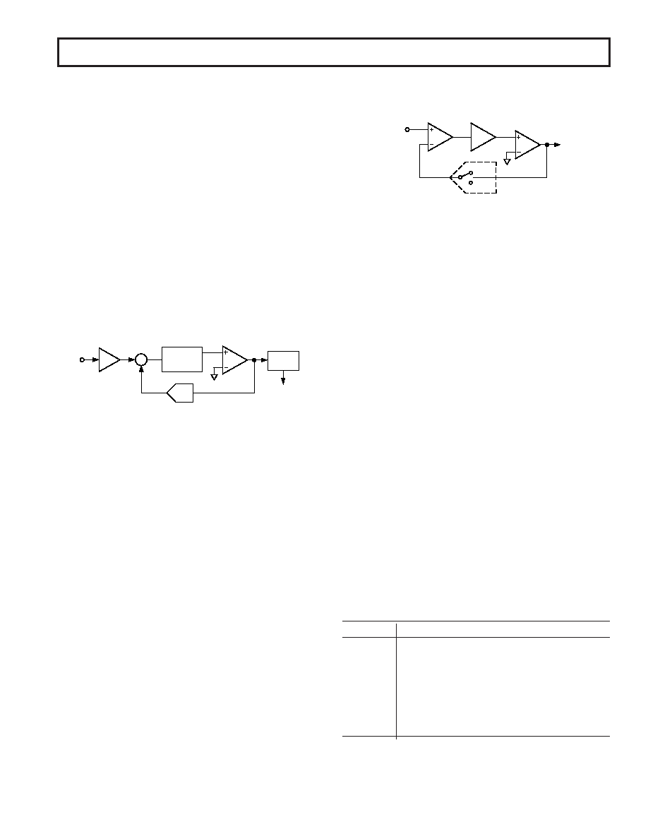
Sigma-delta ADCs are generally described by the order of the
analog low-pass filter. A simple example of a first-order sigma-
delta ADC is shown in Figure 5. This contains only a first-order
low-pass filter or integrator. It also illustrates the derivation of
the alternative name for these devices, charge-balancing ADCs.
DAC
COMPARATOR
+FS
–FS
INTEGRATOR
DIFFERENTIAL
AMPLIFIER
VIN
Figure 5. Basic Charge-Balancing ADC
The device consists of a differential amplifier (whose output is
the difference between the analog input and the output of a
1-bit DAC), an integrator, and a comparator. The term charge-
balancing comes from the fact that this system is a negative
feedback loop that tries to keep the net charge on the integrator
capacitor at zero, by balancing charge injected by the input
voltage with charge injected by the 1-bit DAC. When the analog
input is zero, the only contribution to the integrator output
comes from the 1-bit DAC. For the net charge on the integrator
capacitor to be zero, the DAC output must spend half its time at
+FS and half its time at –FS. Assuming ideal components, the
duty cycle of the comparator will be 50%.
When a positive analog input is applied, the output of the 1-bit
DAC must spend a larger proportion of the time at +FS, so the
duty cycle of the comparator increases. When a negative input
voltage is applied, the duty cycle decreases.
The AD7711 uses a second-order sigma-delta modulator and a
digital filter that provides a rolling average of the sampled out-
put. After power-up, or if there is a step change in the input
voltage, there is a settling time that must elapse before valid
data is obtained.
Input Sample Rate
The modulator sample frequency for the device remains at
fCLK IN/512 (19.5 kHz @ fCLK IN = 10 MHz) regardless of the
selected gain. However, gains greater than
1 are achieved by a
combination of multiple input samples per modulator cycle and
scaling the ratio of reference capacitor to input capacitor. As a
result of the multiple sampling, the input sample rate of
the device varies with the selected gain (see Table III). The
effective input impedance is 1/C
fS where C is the input sam-
pling capacitance and fS is the input sample rate.
Table III. Input Sampling Frequency vs. Gain
Gain
Input Sampling Frequency (fS)
1fCLK IN/256 (39 kHz @ fCLK IN = 10 MHz)
22
fCLK IN/256 (78 kHz @ fCLK IN = 10 MHz)
44
fCLK IN/256 (156 kHz @ fCLK IN = 10 MHz)
88
fCLK IN/256 (312 kHz @ fCLK IN = 10 MHz)
16
8
fCLK IN/256 (312 kHz @ fCLK IN = 10 MHz)
32
8
fCLK IN/256 (312 kHz @ fCLK IN = 10 MHz)
64
8
fCLK IN/256 (312 kHz @ fCLK IN = 10 MHz)
128
8
fCLK IN/256 (312 kHz @ fCLK IN = 10 MHz)
DIGITAL FILTERING
The AD7711’s digital filter behaves like a similar analog filter,
with a few minor differences.
相关PDF资料 |
PDF描述 |
|---|---|
| AD9600ABCPZ-125 | IC ADC 10BIT 125MSPS 64LFCSP |
| ICL3237CAZ | IC 5DRVR/3RCVR RS232 3V 28-SSOP |
| AMIS42665TJAA1G | TRANSCEIVER CAN HS LP 8-SOIC |
| VE-J6W-MY-F2 | CONVERTER MOD DC/DC 5.5V 50W |
| ICL3243ECAZ | IC 3DRVR/5RCVR RS232 3V 28-SSOP |
相关代理商/技术参数 |
参数描述 |
|---|---|
| AD7711ANZ | 制造商:Analog Devices 功能描述:IC ADC 24-BIT SIGMA DELTA |
| AD7711AQ | 功能描述:IC ADC 24BIT RTD I SOURCE 24CDIP RoHS:否 类别:集成电路 (IC) >> 数据采集 - 模数转换器 系列:- 标准包装:1 系列:- 位数:14 采样率(每秒):83k 数据接口:串行,并联 转换器数目:1 功率耗散(最大):95mW 电压电源:双 ± 工作温度:0°C ~ 70°C 安装类型:通孔 封装/外壳:28-DIP(0.600",15.24mm) 供应商设备封装:28-PDIP 包装:管件 输入数目和类型:1 个单端,双极 |
| AD7711AR | 功能描述:IC ADC 24BIT RTD I SOURCE 24SOIC RoHS:否 类别:集成电路 (IC) >> 数据采集 - 模数转换器 系列:- 标准包装:1 系列:- 位数:14 采样率(每秒):83k 数据接口:串行,并联 转换器数目:1 功率耗散(最大):95mW 电压电源:双 ± 工作温度:0°C ~ 70°C 安装类型:通孔 封装/外壳:28-DIP(0.600",15.24mm) 供应商设备封装:28-PDIP 包装:管件 输入数目和类型:1 个单端,双极 |
| AD7711AR-REEL | 功能描述:IC ADC 24BIT RTD I SOURCE 24SOIC RoHS:否 类别:集成电路 (IC) >> 数据采集 - 模数转换器 系列:- 标准包装:1 系列:- 位数:14 采样率(每秒):83k 数据接口:串行,并联 转换器数目:1 功率耗散(最大):95mW 电压电源:双 ± 工作温度:0°C ~ 70°C 安装类型:通孔 封装/外壳:28-DIP(0.600",15.24mm) 供应商设备封装:28-PDIP 包装:管件 输入数目和类型:1 个单端,双极 |
| AD7711AR-REEL7 | 功能描述:IC ADC 24BIT RTD I SOURCE 24SOIC RoHS:否 类别:集成电路 (IC) >> 数据采集 - 模数转换器 系列:- 标准包装:1 系列:- 位数:14 采样率(每秒):83k 数据接口:串行,并联 转换器数目:1 功率耗散(最大):95mW 电压电源:双 ± 工作温度:0°C ~ 70°C 安装类型:通孔 封装/外壳:28-DIP(0.600",15.24mm) 供应商设备封装:28-PDIP 包装:管件 输入数目和类型:1 个单端,双极 |
发布紧急采购,3分钟左右您将得到回复。