- 您现在的位置:买卖IC网 > PDF目录10527 > AD7711ANZ (Analog Devices Inc)IC ADC 24BIT RTD I SOURCE 24-DIP PDF资料下载
参数资料
| 型号: | AD7711ANZ |
| 厂商: | Analog Devices Inc |
| 文件页数: | 6/28页 |
| 文件大小: | 0K |
| 描述: | IC ADC 24BIT RTD I SOURCE 24-DIP |
| 标准包装: | 15 |
| 位数: | 24 |
| 采样率(每秒): | 1.03k |
| 数据接口: | 串行 |
| 转换器数目: | 1 |
| 功率耗散(最大): | 52.5mW |
| 电压电源: | 模拟和数字,双 ± |
| 工作温度: | -40°C ~ 80°C |
| 安装类型: | 通孔 |
| 封装/外壳: | 24-DIP(0.300",7.62mm) |
| 供应商设备封装: | 24-PDIP |
| 包装: | 管件 |
| 输入数目和类型: | 1 个单端,单极;1 个单端,双极;1 个差分,单极;1 个差分,双极 |
| 产品目录页面: | 778 (CN2011-ZH PDF) |
第1页第2页第3页第4页第5页当前第6页第7页第8页第9页第10页第11页第12页第13页第14页第15页第16页第17页第18页第19页第20页第21页第22页第23页第24页第25页第26页第27页第28页
REV. G
–14–
AD7711
First, since digital filtering occurs after the A-to-D conversion
process, it can remove noise injected during the conversion
process. Analog filtering cannot do this.
On the other hand, analog filtering can remove noise super-
imposed on the analog signal before it reaches the ADC. Digital
filtering cannot do this, and noise peaks riding on signals near
full scale have the potential to saturate the analog modulator
and digital filter, even though the average value of the signal is
within limits. To alleviate this problem, the AD7711 has
overrange headroom built into the sigma-delta modulator and
digital filter, which allows overrange excursions of 5% above the
analog input range. If noise signals are larger than this, consid-
eration should be given to analog input filtering, or to reducing
the input channel voltage so that its full scale is half that of the
analog input channel full scale. This will provide an overrange
capability greater than 100% at the expense of reducing the
dynamic range by 1 bit (50%).
Filter Characteristics
The cutoff frequency of the digital filter is determined by the
value loaded to Bits FS0 to FS11 in the control register. At the
maximum clock frequency of 10 MHz, the minimum cutoff
frequency of the filter is 2.58 Hz while the maximum program-
mable cutoff frequency is 269 Hz.
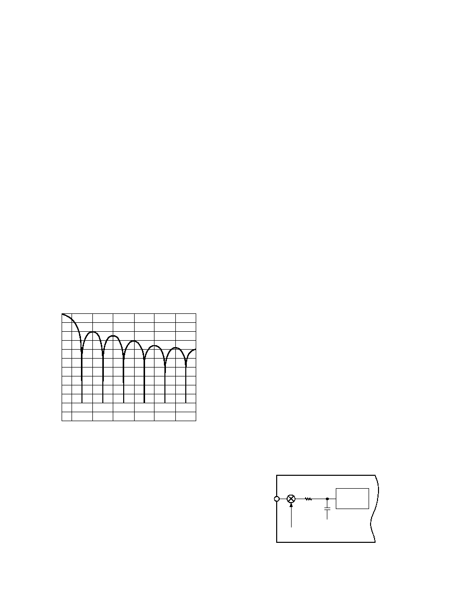
Figure 6 shows the filter frequency response for a cutoff fre-
quency of 2.62 Hz, which corresponds to a first filter notch fre-
quency of 10 Hz. This is a (sinx/x)
3 response (also called sinc3)
that provides >100 dB of 50 Hz and 60 Hz rejection. Program-
ming a different cutoff frequency via FS0–FS11 does not alter
the profile of the filter response; it changes the frequency of the
notches as outlined in the Control Register section.
FREQUENCY – Hz
0
–200
0
GAIN
–
dB
–20
–80
–140
–160
–180
–40
–60
–100
–120
–220
–240
60
10
20
30
40
50
Figure 6. Frequency Response of AD7711 Filter
Since the AD7711 contains this on-chip, low-pass filtering,
there is a settling time associated with step function inputs, and
data on the output will be invalid after a step change until the
settling time has elapsed. The settling time depends upon the
notch frequency chosen for the filter. The output data rate
equates to this filter notch frequency and the settling time of the
filter to a full-scale step input is four times the output data
period. In applications using both input channels, the settling
time of the filter must be allowed to elapse before data from
the second channel is accessed.
Post Filtering
The on-chip modulator provides samples at a 19.5 kHz output
rate. The on-chip digital filter decimates these samples to provide
data at an output rate that corresponds to the programmed first
notch frequency of the filter. Since the output data rate ex-
ceeds the Nyquist criterion, the output rate for a given band-
width will satisfy most application requirements. However,
there may be some applications that require a higher data rate
for a given bandwidth and noise performance. Applications
that need this higher data rate will require some post filtering
following the digital filter of the AD7711.
For example, if the required bandwidth is 7.86 Hz but the required
update rate is 100 Hz, the data can be taken from the AD7711
at the 100 Hz rate giving a –3 dB bandwidth of 26.2 Hz. Post
filtering can be applied to this to reduce the bandwidth and
output noise to the 7.86 Hz bandwidth level, while maintaining
an output rate of 100 Hz.
Post filtering can also be used to reduce the output noise from
the device for bandwidths below 2.62 Hz. At a gain of 128, the
output rms noise is 250 nV. This is essentially device noise or
white noise, and since the input is chopped, the noise has a flat
frequency response. By reducing the bandwidth below 2.62 Hz,
the noise in the resultant pass band can be reduced. A reduction
in bandwidth by a factor of 2 results in a
÷2 reduction in the
output rms noise. This additional filtering will result in a longer
settling time.
Antialias Considerations
The digital filter does not provide any rejection at integer mul-
tiples of the modulator sample frequency (n
19.5 kHz, where
n = 1, 2, 3 . . . ). This means that there are frequency bands,
±f3 dB wide (f3 dB is the cutoff frequency selected by FS0 to FS11),
where noise passes unattenuated to the output. However, due to
the AD7711’s high oversampling ratio, these bands occupy only
a small fraction of the spectrum, and most broadband noise is
filtered. In any case, because of the high oversampling ratio a
simple, RC, single-pole filter is generally sufficient to attenuate
the signals in these bands on the analog input and thus provide
adequate antialiasing filtering.
If passive components are placed in front of the AD7711, care
must be taken to ensure that the source impedance is low enough
so as not to introduce gain errors in the system. The dc input
impedance for the AD7711 is over 1 G
W. The input appears as
a dynamic load that varies with the clock frequency and with the
selected gain (see Figure 7). The input sample rate, as shown
in Table III, determines the time allowed for the analog input
capacitor, CIN, to be charged. External impedances result in a
longer charge time for this capacitor, which may result in gain
errors being introduced on the analog inputs. Table IV shows the
allowable external resistance/capacitance values such that no
gain error to the 16-bit level is introduced while Table V shows
the allowable external resistance/capacitance values such that no
gain error to the 20-bit level is introduced. Both inputs of the
differential input channel (AIN1) look into similar input circuitry.
HIGH
IMPEDANCE
>1G
CINT
11.5pF TYP
VBIAS
RINT
7k
TYP
AIN
SWITCHING FREQUENCY DEPENDS
ON
fCLKIN AND SELECTED GAIN
AD7711
Figure 7. Analog Input Impedance
相关PDF资料 |
PDF描述 |
|---|---|
| AD9600ABCPZ-125 | IC ADC 10BIT 125MSPS 64LFCSP |
| ICL3237CAZ | IC 5DRVR/3RCVR RS232 3V 28-SSOP |
| AMIS42665TJAA1G | TRANSCEIVER CAN HS LP 8-SOIC |
| VE-J6W-MY-F2 | CONVERTER MOD DC/DC 5.5V 50W |
| ICL3243ECAZ | IC 3DRVR/5RCVR RS232 3V 28-SSOP |
相关代理商/技术参数 |
参数描述 |
|---|---|
| AD7711ANZ | 制造商:Analog Devices 功能描述:IC ADC 24-BIT SIGMA DELTA |
| AD7711AQ | 功能描述:IC ADC 24BIT RTD I SOURCE 24CDIP RoHS:否 类别:集成电路 (IC) >> 数据采集 - 模数转换器 系列:- 标准包装:1 系列:- 位数:14 采样率(每秒):83k 数据接口:串行,并联 转换器数目:1 功率耗散(最大):95mW 电压电源:双 ± 工作温度:0°C ~ 70°C 安装类型:通孔 封装/外壳:28-DIP(0.600",15.24mm) 供应商设备封装:28-PDIP 包装:管件 输入数目和类型:1 个单端,双极 |
| AD7711AR | 功能描述:IC ADC 24BIT RTD I SOURCE 24SOIC RoHS:否 类别:集成电路 (IC) >> 数据采集 - 模数转换器 系列:- 标准包装:1 系列:- 位数:14 采样率(每秒):83k 数据接口:串行,并联 转换器数目:1 功率耗散(最大):95mW 电压电源:双 ± 工作温度:0°C ~ 70°C 安装类型:通孔 封装/外壳:28-DIP(0.600",15.24mm) 供应商设备封装:28-PDIP 包装:管件 输入数目和类型:1 个单端,双极 |
| AD7711AR-REEL | 功能描述:IC ADC 24BIT RTD I SOURCE 24SOIC RoHS:否 类别:集成电路 (IC) >> 数据采集 - 模数转换器 系列:- 标准包装:1 系列:- 位数:14 采样率(每秒):83k 数据接口:串行,并联 转换器数目:1 功率耗散(最大):95mW 电压电源:双 ± 工作温度:0°C ~ 70°C 安装类型:通孔 封装/外壳:28-DIP(0.600",15.24mm) 供应商设备封装:28-PDIP 包装:管件 输入数目和类型:1 个单端,双极 |
| AD7711AR-REEL7 | 功能描述:IC ADC 24BIT RTD I SOURCE 24SOIC RoHS:否 类别:集成电路 (IC) >> 数据采集 - 模数转换器 系列:- 标准包装:1 系列:- 位数:14 采样率(每秒):83k 数据接口:串行,并联 转换器数目:1 功率耗散(最大):95mW 电压电源:双 ± 工作温度:0°C ~ 70°C 安装类型:通孔 封装/外壳:28-DIP(0.600",15.24mm) 供应商设备封装:28-PDIP 包装:管件 输入数目和类型:1 个单端,双极 |
发布紧急采购,3分钟左右您将得到回复。