参数资料
| 型号: | AD7716BSZ |
| 厂商: | Analog Devices Inc |
| 文件页数: | 13/16页 |
| 文件大小: | 0K |
| 描述: | IC ADC 22BIT SIGMA-DELTA 44-MQFP |
| 标准包装: | 1 |
| 位数: | 22 |
| 采样率(每秒): | 2.23k |
| 数据接口: | 串行 |
| 转换器数目: | 4 |
| 功率耗散(最大): | 50mW |
| 电压电源: | 模拟和数字,双 ± |
| 工作温度: | -40°C ~ 85°C |
| 安装类型: | 表面贴装 |
| 封装/外壳: | 44-QFP |
| 供应商设备封装: | 44-MQFP(10x10) |
| 包装: | 托盘 |
| 输入数目和类型: | 4 个单端,双极 |
REV. A
AD7716
–6–
ABSOLUTE MAXIMUM RATINGS
1
(TA = +25
°C unless otherwise noted)
AVDD to AGND . . . . . . . . . . . . . . . . . . . . . . . . –0.3 V to +7 V
AVSS to AGND . . . . . . . . . . . . . . . . . . . . . . . +0.3 V to –7 V
AGND to DGND . . . . . . . . . . . . . . . . . . . . . –0.3 V to +0.3 V
AVDD to DVDD . . . . . . . . . . . . . . . . . . . . . . . –0.3 V to +0.3 V
Analog Inputs to AGND . . . . . . AVSS – 0.3 V to AVDD + 0.3 V
VREF to AGND . . . . . . . . . . . . AVSS – 0.3 V to AVDD + 0.3 V
Digital Inputs to DGND
2
. . . . . . . . . . –0.3 V to DVDD + 0.3 V
Digital Outputs to DGND . . . . . . . . . . –0.3 V to DVDD + 0.3 V
Operating Temperature Range
Commercial Plastic (B Versions) . . . . . . . . . . . –40
°C to +85°C
Storage Temperature Range . . . . . . . . . . . . . –65
°C to +150°C
PQFP Package, Power Dissipation . . . . . . . . . . . . . . . 450 mW
θ
JA Thermal Impedance . . . . . . . . . . . . . . . . . . . . . . 95
°C/W
Lead Temperature, Soldering
Vapor Phase (60 sec) . . . . . . . . . . . . . . . . . . . . . . +215
°C
Infrared (15 sec) . . . . . . . . . . . . . . . . . . . . . . . . . . +220
°C
PLCC Package, Power Dissipation . . . . . . . . . . . . . . . 500 mW
θ
JA Thermal Impedance . . . . . . . . . . . . . . . . . . . . . . 55
°C/W
Lead Temperature, Soldering
Vapor Phase (60 sec) . . . . . . . . . . . . . . . . . . . . . . +215
°C
Infrared (15 sec) . . . . . . . . . . . . . . . . . . . . . . . . . . +220
°C
NOTES
1Stresses above those listed under “Absolute Maximum Ratings” may cause
permanent damage to the device. This is a stress rating only and functional
operation of the device at these or any other conditions above those listed in the
operational sections of this specification is not implied. Exposure to absolute
maximum rating conditions for extended periods may affect device reliability.
2Transient currents of up to 100 mA will not cause SCR latch-up.
CAUTION
ESD (electrostatic discharge) sensitive device. Electrostatic charges as high as 4000 V readily
accumulate on the human body and test equipment and can discharge without detection.
Although these devices feature proprietary ESD protection circuitry, permanent damage may
occur on devices subjected to high energy electrostatic discharges. Therefore, proper ESD
precautions are recommended to avoid performance degradation or loss of functionality.
WARNING!
ESD SENSITIVE DEVICE
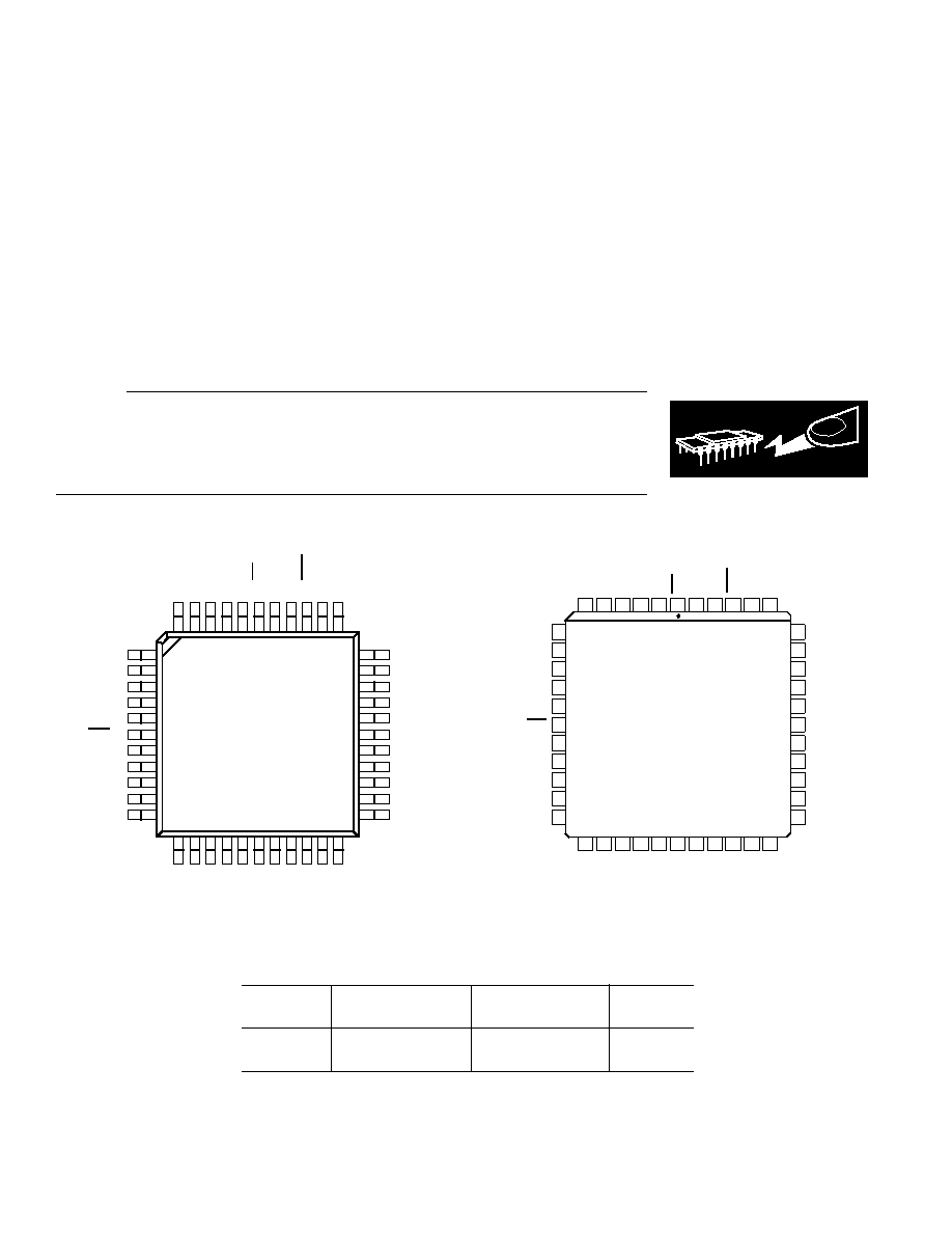
PQFP PINOUT
PLCC PINOUT
NC = NO CONNECT
MODE
NC
DIN1
NC
CASCIN
NC
DVDD
NC
RFS
SCLK
DOUT1
DGND
NC
CLKIN
D
OUT
2
DGND
NC
A2
AGND
A
IN
3
AGND
A
IN
2
CLKOUT
SDATA
NC
AGND
A
IN
4
A0
A1
NC
VREF
AVSS
AGND
CASCOUT
AGND
AVDD
AIN1
RESET
44
1
2
64
5
21
24
23
22
18
20
19
39
38
35
34
33
37
36
3
7
8
11
12
13
9
10
40
41
42
25
28
27
26
43
31
30
29
32
15
16
17
14
TOP VIEW
(Not to Scale)
AD7716
A2
AGND
TFS
DRDY
26 CASCOUT
NC = NO CONNECT
AGND
12
A2
13
AGND
14
A
IN
2
15
AGND
16
A
IN
3
17
AGND
18
A1
19
AGND
20
A
IN
4
21
A0
22
44
NC
43
CLKIN
42
NC
41
CLKOUT
40
D
OUT
2
38
DGND
37
NC
35
SDATA
34
NC
33 MODE
32 NC
31 NC
30 DVDD
29 DIN1
28 NC
27 CASCIN
25 VREF
24 AVSS
23 AGND
NC 1
NC 2
DOUT1 3
DGND 4
NC 5
SCLK 7
RESET 8
AGND 9
AVDD 10
AIN1 11
AD7716
TOP VIEW
(Not to Scale)
RFS 6
36
DRDY
39
TFS
ORDERING GUIDE
Temperature
Output Noise
Package
Model
Range
(Filter: 146 Hz)
Option*
AD7716BP
–40
°C to +85°C
11
V rms
P-44A
AD7716BS
–40
°C to +85°C
11
V rms
S-44
*P = PLCC (Plastic Leaded Chip Carrier); S = PQFP (Plastic Quad Flatpack).
相关PDF资料 |
PDF描述 |
|---|---|
| AD7718BRU-REEL7 | IC ADC 24BIT R-R 8/10CH 28-TSSOP |
| AD7719BRZ | IC ADC 16BIT 24BIT DUAL 28SOIC |
| AD7720BRU | IC MODULATOR SIGMA-DELTA 28TSSOP |
| AD7721AR | IC ADC 16BIT SIGMA-DELTA 28-SOIC |
| AD7722ASZ | IC ADC 16BIT 195KSPS 44-MQFP |
相关代理商/技术参数 |
参数描述 |
|---|---|
| AD7716-DF | 功能描述:IC ADC 22BIT SIGMA-DELTA 制造商:analog devices inc. 系列:- 零件状态:上次购买时间 标准包装:1 |
| AD7718 | 制造商:AD 制造商全称:Analog Devices 功能描述:8-/10-Channel, Low Voltage, Low Power, ADCs |
| AD7718BR | 功能描述:IC ADC 24BIT R-R 8/10CH 28-SOIC RoHS:否 类别:集成电路 (IC) >> 数据采集 - 模数转换器 系列:- 产品培训模块:Lead (SnPb) Finish for COTS Obsolescence Mitigation Program 标准包装:2,500 系列:- 位数:12 采样率(每秒):3M 数据接口:- 转换器数目:- 功率耗散(最大):- 电压电源:- 工作温度:- 安装类型:表面贴装 封装/外壳:SOT-23-6 供应商设备封装:SOT-23-6 包装:带卷 (TR) 输入数目和类型:- |
| AD7718BR-REEL | 功能描述:IC ADC 24BIT R-R 8/10CH 28-SOIC RoHS:否 类别:集成电路 (IC) >> 数据采集 - 模数转换器 系列:- 标准包装:1,000 系列:- 位数:16 采样率(每秒):45k 数据接口:串行 转换器数目:2 功率耗散(最大):315mW 电压电源:模拟和数字 工作温度:0°C ~ 70°C 安装类型:表面贴装 封装/外壳:28-SOIC(0.295",7.50mm 宽) 供应商设备封装:28-SOIC W 包装:带卷 (TR) 输入数目和类型:2 个单端,单极 |
| AD7718BR-REEL7 | 制造商:Analog Devices 功能描述:ADC Single Delta-Sigma 1.365ksps 24-bit Serial 28-Pin SOIC W T/R 制造商:Analog Devices 功能描述:ADC SGL DELTA-SIGMA 1.365KSPS 24BIT SERL 28SOIC W - Tape and Reel 制造商:Rochester Electronics LLC 功能描述:4/5 CHNL DIFF OR 8/10 CHNL 24-BIT ADC - Tape and Reel |
发布紧急采购,3分钟左右您将得到回复。