参数资料
| 型号: | AD7716BSZ |
| 厂商: | Analog Devices Inc |
| 文件页数: | 7/16页 |
| 文件大小: | 0K |
| 描述: | IC ADC 22BIT SIGMA-DELTA 44-MQFP |
| 标准包装: | 1 |
| 位数: | 22 |
| 采样率(每秒): | 2.23k |
| 数据接口: | 串行 |
| 转换器数目: | 4 |
| 功率耗散(最大): | 50mW |
| 电压电源: | 模拟和数字,双 ± |
| 工作温度: | -40°C ~ 85°C |
| 安装类型: | 表面贴装 |
| 封装/外壳: | 44-QFP |
| 供应商设备封装: | 44-MQFP(10x10) |
| 包装: | 托盘 |
| 输入数目和类型: | 4 个单端,双极 |
REV. A
–15–
AD7716
The optimum setup for reading all four channels of the AD7716
into the DSP56001 is six 24-bit reads. This will provide 144 clock
edges to shift out the 128 bits of data in the AD7716 output shift
register. The first clock applied to the AD7716 will clock out
DB21 of A
IN1.
DRDY
from the AD7716 can be used as an
interrupt input to the DSP56001 to control the data transfer.
Either IRQA or IRQB of the DSP56001 can be used to detect the
interrupt.
DSP56001
+5V
AD7716
CASCOUT
CASCIN
RESET
CONTROL
SC2
SC1
SCK
SC0
STD
SRD
IRQ
MODE
TFS
RFS
SCLK
SDATA
DRDY
Figure 10. DSP56001 Interface
TMS320C25 Interface
Figure 11 shows the AD7716 interfaced to the TMS320C25
DSP using the master mode interface. For initial programming
of the AD7716 control register, the external gated clock is re-
quired. FSX going low enables this. When the two 8-bit bytes
have been sent to the AD7716, the FSX should go permanently
high. The external gated clock will now be disabled and the
AD7716 will take control of the SDATA line. It will begin
transmitting data as soon as it becomes available. It also pro-
vides the clock and frame synchronization signals required by
the DSP.
Reset for the AD7716 is provided by one of the DSP flag
outputs.
FLAG
OUTPUT
FSR
DR
DT
FSX
CLKR
CLKX
MODE
RFS
RESET
CASCIN
AD7716
CASCOUT
TMS320C25
GATED
CLOCK
EN
RESET CONTROL
SDATA
TFS
SCLK
Figure 11. TMS320C25 to AD7716 Interface
When the AD7716 is programmed for the maximum cutoff fre-
quency of 584 Hz, the output data rate is 2.25 kHz. This
means that there is 440
s available to read the data and do the
necessary number crunching before the next sample must be
read. Assuming that the ADSP-2101 is running from a master
clock of 12.5 MHz means that the maximum SCLK available is
6.25 MHz (1/2 the master clock frequency). It will then take 40
s to transfer the 256 bits of data from the ADC to the DSP.
This leaves 400
s for number crunching in the DSP. If the
programmed cutoff frequency is lower then this allows even
more time to the DSP.
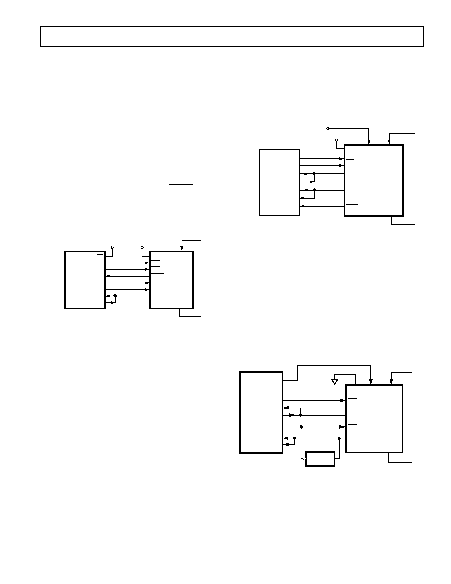
MC68HC11 Interface
The MC68HC11 microcomputer can be interfaced to the
AD7716 using the slave mode interface. Figure 9 shows a typi-
cal setup. The MODE pin on the AD7716 is tied high for slave
mode operation. The SPI port of the MC68HC11 is used. The
microcomputer is in its single chip mode.
DRDY
from the
AD7716 is connected to the IRQ input of the MC68HC11.
MISO and MOSI on the MC68HC11 should be configured for
wired-or operation. Depending on the interface configuration,
it may be necessary to provide bidirectional buffers between
these lines.
PC0
PC1
PC2
PC3
SCK
MISO
MOSI
SS
MC68HC11
MODE
RFS
TFS
DRDY
RESET
SCLK
SDATA
AD7716
+5V
CASCOUT
CASCIN
PC0
PC1
IRQ
PC2
SCK
MISO
MOSI
SS
MC68HC11
MODE
RFS
TFS
DRDY
RESET
SCLK
SDATA
AD7716
+5V
CASCOUT
CASCIN
Figure 9. MC68HC11 to AD7716 Interface
The MC68HC11 is configured in the master mode with its
CPOL bit set to a logic zero and its CPHA bit set to a logic one.
With an 8 MHz CLKIN input on the AD7716, the device will
operate with all four serial clock rates of the MC68HC11.
Sixteen, 8-bit read operations are necessary to read the 128 bits
from the AD7716 output register. An extra read is necessary to
reset the output register. This means a total of 17 read opera-
tions are needed from the MC68HC11.
DSP56001 Interface
Figure 10 shows an interface to the DSP56001 digital signal
processor. The AD7716 is set up for the slave interface mode.
The DSP56001 is set up for asynchronous operation with gated
clock and normal framing. Data must be written to the
AD7716 control register in two 8-bit bytes. The first byte is
written to the DSP56001 SSI transmit data register (TX) and
this is automatically transferred to the transmit shift register
when the frame sync occurs. Data is shifted out to the STD pin
by the internal bit clock (SCK) when the associated frame sync
output is asserted.
相关PDF资料 |
PDF描述 |
|---|---|
| AD7718BRU-REEL7 | IC ADC 24BIT R-R 8/10CH 28-TSSOP |
| AD7719BRZ | IC ADC 16BIT 24BIT DUAL 28SOIC |
| AD7720BRU | IC MODULATOR SIGMA-DELTA 28TSSOP |
| AD7721AR | IC ADC 16BIT SIGMA-DELTA 28-SOIC |
| AD7722ASZ | IC ADC 16BIT 195KSPS 44-MQFP |
相关代理商/技术参数 |
参数描述 |
|---|---|
| AD7716-DF | 功能描述:IC ADC 22BIT SIGMA-DELTA 制造商:analog devices inc. 系列:- 零件状态:上次购买时间 标准包装:1 |
| AD7718 | 制造商:AD 制造商全称:Analog Devices 功能描述:8-/10-Channel, Low Voltage, Low Power, ADCs |
| AD7718BR | 功能描述:IC ADC 24BIT R-R 8/10CH 28-SOIC RoHS:否 类别:集成电路 (IC) >> 数据采集 - 模数转换器 系列:- 产品培训模块:Lead (SnPb) Finish for COTS Obsolescence Mitigation Program 标准包装:2,500 系列:- 位数:12 采样率(每秒):3M 数据接口:- 转换器数目:- 功率耗散(最大):- 电压电源:- 工作温度:- 安装类型:表面贴装 封装/外壳:SOT-23-6 供应商设备封装:SOT-23-6 包装:带卷 (TR) 输入数目和类型:- |
| AD7718BR-REEL | 功能描述:IC ADC 24BIT R-R 8/10CH 28-SOIC RoHS:否 类别:集成电路 (IC) >> 数据采集 - 模数转换器 系列:- 标准包装:1,000 系列:- 位数:16 采样率(每秒):45k 数据接口:串行 转换器数目:2 功率耗散(最大):315mW 电压电源:模拟和数字 工作温度:0°C ~ 70°C 安装类型:表面贴装 封装/外壳:28-SOIC(0.295",7.50mm 宽) 供应商设备封装:28-SOIC W 包装:带卷 (TR) 输入数目和类型:2 个单端,单极 |
| AD7718BR-REEL7 | 制造商:Analog Devices 功能描述:ADC Single Delta-Sigma 1.365ksps 24-bit Serial 28-Pin SOIC W T/R 制造商:Analog Devices 功能描述:ADC SGL DELTA-SIGMA 1.365KSPS 24BIT SERL 28SOIC W - Tape and Reel 制造商:Rochester Electronics LLC 功能描述:4/5 CHNL DIFF OR 8/10 CHNL 24-BIT ADC - Tape and Reel |
发布紧急采购,3分钟左右您将得到回复。