- 您现在的位置:买卖IC网 > PDF目录10278 > AD7718BR-REEL (Analog Devices Inc)IC ADC 24BIT R-R 8/10CH 28-SOIC PDF资料下载
参数资料
| 型号: | AD7718BR-REEL |
| 厂商: | Analog Devices Inc |
| 文件页数: | 26/44页 |
| 文件大小: | 0K |
| 描述: | IC ADC 24BIT R-R 8/10CH 28-SOIC |
| 标准包装: | 1,000 |
| 位数: | 24 |
| 采样率(每秒): | 1.37k |
| 数据接口: | DSP,MICROWIRE?,QSPI?,串行,SPI? |
| 转换器数目: | 1 |
| 功率耗散(最大): | 3.84mW |
| 电压电源: | 模拟和数字 |
| 工作温度: | -40°C ~ 85°C |
| 安装类型: | 表面贴装 |
| 封装/外壳: | 28-SOIC(0.295",7.50mm 宽) |
| 供应商设备封装: | 28-SOIC W |
| 包装: | 带卷 (TR) |
| 输入数目和类型: | 5 个差分,单极;5 个差分,双极;10 伪差分,单极;10 伪差分,双极 |
| 配用: | EVAL-AD7718EBZ-ND - BOARD EVALUATION FOR AD7718 |
第1页第2页第3页第4页第5页第6页第7页第8页第9页第10页第11页第12页第13页第14页第15页第16页第17页第18页第19页第20页第21页第22页第23页第24页第25页当前第26页第27页第28页第29页第30页第31页第32页第33页第34页第35页第36页第37页第38页第39页第40页第41页第42页第43页第44页
REV. 0
–32–
AD7708/AD7718
Configuring the AD7708/AD7718
All user-accessible registers on the AD7708 and AD7718 are
accessed via the serial interface. Communication with any of
these registers is initiated by first writing to the Communica-
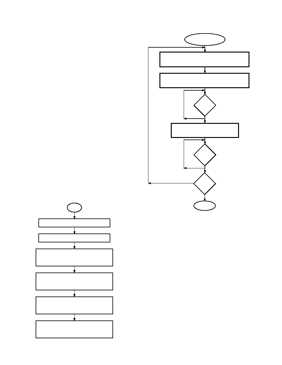
tions Register. Figures 16, 17, and 18 show flow diagrams for
initializing the ADC, a sequence for calibrating the ADC chan-
nels, and a routine that cycles through and reads all channels.
Figure 16 shows a flowchart detailing necessary programming
steps required to initialize the ADC. The following are the general
programming steps required:
1. Configure and initialize the microcontroller or microprocessor
serial port.
2. Initialize the AD7708/AD7718 by configuring the following
registers:
a. IOCON to configure the digital I/O port.
b. FILTER to configure the update rate for each channel.
c. ADCCON to select the active input channel, select
the analog input range, and select unipolar or bipolar
operation.
d. MODE to configure the operating mode. The mode
register selects chop or nonchop operation, buffered/
unbuffered operation of the AINCOM input, 8-/10-
channel mode of operation and reference select along
with the selection of conversion, calibration or idle
modes of operation.
All operations consist of a write to the communications register
to specify the next operation as a write to a specified register.
Data is then written to the specified register. When each sequence
is complete, the ADC defaults to waiting for another write to
the communications register to specify the next operation.
WRITE TO COMMUNICATIONS REGISTER SETTING UP
NEXT OPERATION TO BE A WRITE TO THE MODE
REGISTER. CALIBRATE AND SELECT MODE OF
OPERATION
WRITE TO COMMUNICATIONS REGISTER SETTING UP
NEXT OPERATION TO BE A WRITE TO THE ADC
CONTROL REGISTER. CONFIGURE ADCCON
WRITE TO COMMUNICATIONS REGISTER SETTING UP
NEXT OPERATION TO BE A WRITE TO THE FILTER
REGISTER. SET SF WORD FOR REQUIRED
UPDATE RATE
WRITE TO COMMUNICATIONS REGISTER SELECTING
NEXT OPERATION TO BE A WRITE TO THE IOCON
REGISTER AND CONFIGURE THIS REGISTER
POWER-ON/RESET FOR AD7708/AD7718
CONFIGURE AND INITIALIZE
C/ P SERIAL PORT
START
Figure 16. Initializing AD7708/AD7718
END
CAL
ANOTHER
CHANNEL
WRITE TO MODE REGISTER SELECTING
FULL-SCALE CALIBRATION
WRITE TO MODE REGISTER SELECTING
ZERO-SCALE CALIBRATION
WRITE TO ADCCON SELECTING CHANNEL AND CONFIGURING
INPUT RANGE AND UNIPOLAR/BIPOLAR MODE
CALIBRATION ROUTINE
MD BITS
= 001?
NO
YES
MD BITS
= 001?
NO
YES
NO
Figure 17. Calibrating the AD7708/AD7718
Figure 17 shows a flowchart detailing necessary programming
steps required when calibrating the AD7708/AD7718. The
AD7708/AD7718 have dedicated calibration register pairs for
each of the fully-differential input channels. Having a dedicated
register pair per channel allows each channel to be calibrated as
part of the initialization and the ADC picks up the relevant
coefficients for each channel during normal operation. When
operating is pseudo-differential mode channels share calibration
register pairs. Channels that share coefficients should be config-
ured with the same operating conditions to avoid having to
calibrate each time a channel is switched, especially with chop
mode disabled. The AD7708/AD7718 are factory-calibrated
with chop mode enabled and, therefore, if the ADC is operated
at the same conditions as the factory-calibration field calibra-
tions will not be required. Extremely low offset error and offset
and gain drift errors are a by product of the chopping scheme.
When operating with chop mode disabled, the user can achieve
faster throughput times. An offset calibration is required with
chop disabled when a gain or temperature change occurs. The
following are the general programming steps required when
calibrating a channel on the AD7708/AD7718.
相关PDF资料 |
PDF描述 |
|---|---|
| D38999/24WJ24BN | CONN HSG RCPT 24POS JAM NUT SCKT |
| D38999/20KC98AN | CONN HSG RCPT 10POS WALL MT PINS |
| MS27473T10A99PB | CONN PLUG 7POS STRAIGHT W/PINS |
| AD7495BRZ-REEL7 | IC ADC 12BIT SRL LP W/REF 8-SOIC |
| SL404MX | CONN PLUG 4POS MALE W/COUPLING |
相关代理商/技术参数 |
参数描述 |
|---|---|
| AD7718BR-REEL7 | 制造商:Analog Devices 功能描述:ADC Single Delta-Sigma 1.365ksps 24-bit Serial 28-Pin SOIC W T/R 制造商:Analog Devices 功能描述:ADC SGL DELTA-SIGMA 1.365KSPS 24BIT SERL 28SOIC W - Tape and Reel 制造商:Rochester Electronics LLC 功能描述:4/5 CHNL DIFF OR 8/10 CHNL 24-BIT ADC - Tape and Reel |
| AD7718BRU | 功能描述:IC ADC 24BIT R-R 8/10CH 28-TSSOP RoHS:否 类别:集成电路 (IC) >> 数据采集 - 模数转换器 系列:- 标准包装:1,000 系列:- 位数:12 采样率(每秒):300k 数据接口:并联 转换器数目:1 功率耗散(最大):75mW 电压电源:单电源 工作温度:0°C ~ 70°C 安装类型:表面贴装 封装/外壳:24-SOIC(0.295",7.50mm 宽) 供应商设备封装:24-SOIC 包装:带卷 (TR) 输入数目和类型:1 个单端,单极;1 个单端,双极 |
| AD7718BRU-REEL | 功能描述:IC ADC 24BIT R-R 8/10CH 28-TSSOP RoHS:否 类别:集成电路 (IC) >> 数据采集 - 模数转换器 系列:- 标准包装:1,000 系列:- 位数:16 采样率(每秒):45k 数据接口:串行 转换器数目:2 功率耗散(最大):315mW 电压电源:模拟和数字 工作温度:0°C ~ 70°C 安装类型:表面贴装 封装/外壳:28-SOIC(0.295",7.50mm 宽) 供应商设备封装:28-SOIC W 包装:带卷 (TR) 输入数目和类型:2 个单端,单极 |
| AD7718BRU-REEL7 | 功能描述:IC ADC 24BIT R-R 8/10CH 28-TSSOP RoHS:否 类别:集成电路 (IC) >> 数据采集 - 模数转换器 系列:- 产品培训模块:Lead (SnPb) Finish for COTS Obsolescence Mitigation Program 标准包装:2,500 系列:- 位数:12 采样率(每秒):3M 数据接口:- 转换器数目:- 功率耗散(最大):- 电压电源:- 工作温度:- 安装类型:表面贴装 封装/外壳:SOT-23-6 供应商设备封装:SOT-23-6 包装:带卷 (TR) 输入数目和类型:- |
| AD7718BRUZ | 功能描述:IC ADC 24BIT R-R 8/10CH 28-TSSOP RoHS:是 类别:集成电路 (IC) >> 数据采集 - 模数转换器 系列:- 标准包装:1 系列:microPOWER™ 位数:8 采样率(每秒):1M 数据接口:串行,SPI? 转换器数目:1 功率耗散(最大):- 电压电源:模拟和数字 工作温度:-40°C ~ 125°C 安装类型:表面贴装 封装/外壳:24-VFQFN 裸露焊盘 供应商设备封装:24-VQFN 裸露焊盘(4x4) 包装:Digi-Reel® 输入数目和类型:8 个单端,单极 产品目录页面:892 (CN2011-ZH PDF) 其它名称:296-25851-6 |
发布紧急采购,3分钟左右您将得到回复。