参数资料
| 型号: | AD7719BRZ |
| 厂商: | Analog Devices Inc |
| 文件页数: | 22/40页 |
| 文件大小: | 0K |
| 描述: | IC ADC 16BIT 24BIT DUAL 28SOIC |
| 标准包装: | 27 |
| 位数: | 16/24 |
| 采样率(每秒): | 105 |
| 数据接口: | DSP,MICROWIRE?,QSPI?,串行,SPI? |
| 转换器数目: | 2 |
| 功率耗散(最大): | 4.5mW |
| 电压电源: | 模拟和数字 |
| 工作温度: | -40°C ~ 85°C |
| 安装类型: | 表面贴装 |
| 封装/外壳: | 28-SOIC(0.295",7.50mm 宽) |
| 供应商设备封装: | 28-SOIC W |
| 包装: | 管件 |
| 输入数目和类型: | 3 个差分,单极;3 个差分,双极 |
第1页第2页第3页第4页第5页第6页第7页第8页第9页第10页第11页第12页第13页第14页第15页第16页第17页第18页第19页第20页第21页当前第22页第23页第24页第25页第26页第27页第28页第29页第30页第31页第32页第33页第34页第35页第36页第37页第38页第39页第40页
REV. A
AD7719
–29–
AD7719-to-68HC11 Interface
Figure 12 shows an interface between the AD7719 and the 68HC11
microcontroller. The diagram shows the minimum (3-wire) inter-
face with
CS on the AD7719 hardwired low. In this scheme, the
RDY bits of the Status register are monitored to determine
when the Data register is updated. RDY0 indicates the status of
the main ADC channel while RDY1 indicates the status of the
aux channel. An alternative scheme, which increases the number
of interface lines to four, is to monitor the
RDY output line
from the AD7719. The monitoring of the
RDY line can be done in
two ways. First,
RDY can be connected to one of the 68HC11’s
port bits (such as PC0), which is configured as an input. This
port bit is then polled to determine the status of
RDY. The
second scheme is to use an interrupt driven system, in which case
the
RDY output is connected to the IRQ input of the 68HC11. For
interfaces that require control of the
CS input on the AD7719,
one of the port bits of the 68HC11 (such as PC1) that is
configured as an output, can be used to drive the
CS input.
The 68HC11 is configured in the master mode with its CPOL
bit set to a logic 1 and its CPHA bit set to a logic 1. When the
68HC11 is configured like this, its SCLK line idles high between
data transfers. The AD7719 is not capable of full duplex opera-
tion. If the AD7719 is configured for a write operation, no data appears
on the DOUT lines even when the SCLK input is active. Simi-
larly, if the AD7719 is configured for a read operation, data
presented to the part on the DIN line is ignored even when
SCLK is active.
68HC11
AD7719
VDD
SS
SCK
MISO
MOSI
RESET
SCLK
CS
DIN
DOUT
VDD
Figure 12. AD7719-to-68HC11 Interface
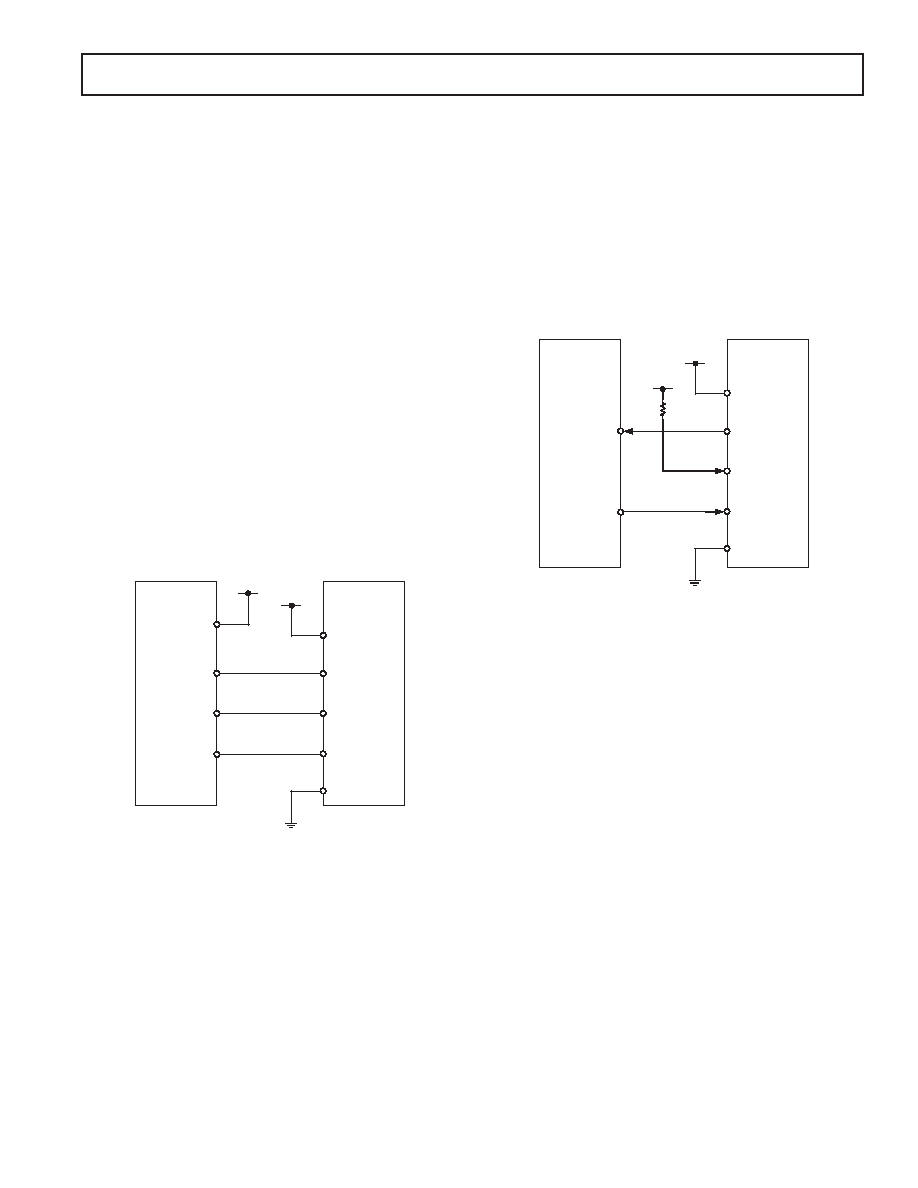
AD7719-to-8xC51 Interface
An interface circuit between the AD7719 and the 8xC51 microcon-
troller is shown in Figure 13. The diagram shows the minimum
number of interface connections with
CS on the AD7719 hard-
wired low. In the case of the 8xC51 interface, the minimum
number of interconnects is just two. In this scheme, the RDY
bits of the Status register are monitored to determine when the
Data register is updated. The alternative scheme, which increases
the number of interface lines to three, is to monitor the
RDY output
line from the AD7719. The monitoring of the
RDY line can be
done in two ways. First,
RDY can be connected to one of the
8xC51’s port bits (such as P1.0) that is configured as an input.
This port bit is then polled to determine the status of
RDY.
DVDD
8xC51
AD7719
P3.0
P3.1
RESET
SCLK
CS
DVDD
10k
DIN
DOUT
Figure 13. AD7719-to-8XC51 Interface
The second scheme is to use an interrupt-driven system, in which
case the
RDY output is connected to the INT1 input of the
8xC51. For interfaces that require control of the
CS input on
the AD7719, one of the port bits of the 8xC51 (such as P1.1)
that is configured as an output can be used to drive the
CS
input. The 8xC51 is configured in its Mode 0 serial interface
mode. Its serial interface contains a single data line. As a result,
the DOUT and DIN pins of the AD7719 should be connected
together with a 10 k
pull-up resistor. The serial clock on the
8xC51 idles high between data transfers. The 8xC51 outputs the
LSB first in a write operation, while the AD7719 expects the
MSB first so the data to be transmitted has to be rearranged
before being written to the output serial register. Similarly, the
AD7719 outputs the MSB first during a read operation while
the 8xC51 expects the LSB first. Therefore, the data read into
the serial buffer needs to be rearranged before the correct data
word from the AD7719 is available in the accumulator.
相关PDF资料 |
PDF描述 |
|---|---|
| AD7720BRU | IC MODULATOR SIGMA-DELTA 28TSSOP |
| AD7721AR | IC ADC 16BIT SIGMA-DELTA 28-SOIC |
| AD7722ASZ | IC ADC 16BIT 195KSPS 44-MQFP |
| AD7723BSZ-REEL | IC ADC 16BIT SIGMA-DELTA 44MQFP |
| AD7725BSZ | IC ADC 16BIT PROG 44MQFP |
相关代理商/技术参数 |
参数描述 |
|---|---|
| AD7720 | 制造商:AD 制造商全称:Analog Devices 功能描述:CMOS Sigma-Delta Modulator |
| AD7720BRU | 功能描述:IC MODULATOR SIGMA-DELTA 28TSSOP RoHS:否 类别:集成电路 (IC) >> 数据采集 - 模数转换器 系列:- 标准包装:1,000 系列:- 位数:12 采样率(每秒):300k 数据接口:并联 转换器数目:1 功率耗散(最大):75mW 电压电源:单电源 工作温度:0°C ~ 70°C 安装类型:表面贴装 封装/外壳:24-SOIC(0.295",7.50mm 宽) 供应商设备封装:24-SOIC 包装:带卷 (TR) 输入数目和类型:1 个单端,单极;1 个单端,双极 |
| AD7720BRU-REEL | 制造商:Analog Devices 功能描述:ADC Single Delta-Sigma 25Msps 16-bit Serial 28-Pin TSSOP T/R |
| AD7720BRU-REEL7 | 制造商:Analog Devices 功能描述:ADC Single Delta-Sigma 25Msps 16-bit Serial 28-Pin TSSOP T/R 制造商:Rochester Electronics LLC 功能描述:- Tape and Reel |
| AD7720BRUZ | 功能描述:IC MODULATOR SIGMA-DELTA 28TSSOP RoHS:是 类别:集成电路 (IC) >> 数据采集 - 模数转换器 系列:- 标准包装:1,000 系列:- 位数:12 采样率(每秒):300k 数据接口:并联 转换器数目:1 功率耗散(最大):75mW 电压电源:单电源 工作温度:0°C ~ 70°C 安装类型:表面贴装 封装/外壳:24-SOIC(0.295",7.50mm 宽) 供应商设备封装:24-SOIC 包装:带卷 (TR) 输入数目和类型:1 个单端,单极;1 个单端,双极 |
发布紧急采购,3分钟左右您将得到回复。