- 您现在的位置:买卖IC网 > PDF目录1983 > AD7767BRUZ-RL7 (Analog Devices Inc)ADC 24BIT 15MW 128KSPS 16TSSOP PDF资料下载
参数资料
| 型号: | AD7767BRUZ-RL7 |
| 厂商: | Analog Devices Inc |
| 文件页数: | 14/25页 |
| 文件大小: | 0K |
| 描述: | ADC 24BIT 15MW 128KSPS 16TSSOP |
| 标准包装: | 1,000 |
| 位数: | 24 |
| 采样率(每秒): | 128k |
| 数据接口: | 串行 |
| 转换器数目: | 1 |
| 功率耗散(最大): | 18mW |
| 电压电源: | 模拟和数字 |
| 工作温度: | -40°C ~ 105°C |
| 安装类型: | 表面贴装 |
| 封装/外壳: | 16-TSSOP(0.173",4.40mm 宽) |
| 供应商设备封装: | 16-TSSOP |
| 包装: | 带卷 (TR) |
| 输入数目和类型: | 1 个差分,单极 |
| 配用: | EVAL-AD7767EDZ-ND - BOARD EVAL AD7767 128KSPS 108DB EVAL-AD7767-1EDZ-ND - BOARD EVAL AD7767-1 64KSPS 111DB |
AD7767
Rev. C | Page 20 of 2
4
DRIVING THE AD7767
R1 and R2 set the attenuation ratio between the input range and
the ADC range (VREF). R1, R2, and CF are chosen depending on
the desired input resistance, signal bandwidth, antialiasing, and
noise contribution. The ratio of R2 to R1 should be equal to the
ratio of REF to the peak-to-peak input voltage. For example, for
the ±10 V range with a 4 kΩ impedance, R2 = 1 kΩ and R1 = 4 kΩ.
The AD7767 must be driven with fully differential inputs. The
common-mode voltage of the differential inputs to the AD7767
device and therefore the limits on the differential inputs are set
by the reference voltage (VREF) applied to the device. The common-
mode voltage of the AD7767 is VREF/2. When the AD7767 VREF+ pin
common mode is at 2.5 V, meaning that the maximum inputs that
can be applied on the AD7767 differential inputs are a 5 V p-p
input around 2.5 V.
R3 and R4 set the common mode on the IN input, and R5 and R6
set the common mode on the IN+ input of the ADC. The common
mode, which is equal to the voltage present at VOFFSET1, should be
close to VREF/2. The voltage present should roughly be set to the
ratio of VOFFSET1 to 1 + R2/R1.
06
85
9-
01
6
0V
VIN+
VIN–
VREF
2
0V
VREF
2
06
85
9-
02
0
ADA4841-1
15
3.3nF
1k
ADA4841-1
15
3.3nF
1k
4
5
1
2
AD7767
AVDD
VREF+
VIN+
VIN–
2.2nF
*
ADR4xx
ADP3330-2.5
2.5V
2.5V TO 5V
REFERENCE
VOLTAGE
1k
1k
1k
1k
AIN+
AIN–
*SEE VREF+ INPUT SIGNAL SECTION FOR DETAILS.
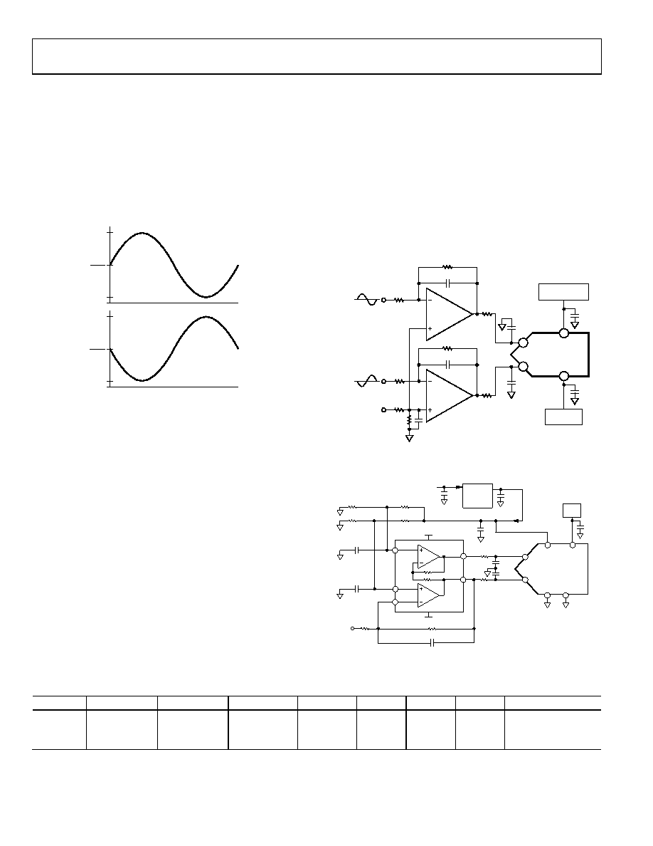
Figure 39. Maximum Differential Inputs to the AD7767
An analog voltage of 2.5 V supplies the AD7767 AVDD pin.
However, the AD7767 allows the user to apply a reference
voltage of up to 5 V. This provides the user with an increased
full-scale range, offering the user the option of using the
AD7767 with a greater LSB voltage. Figure 39 shows the
maximum inputs to the AD7767.
Figure 40. Driving the AD7767 from a Fully Differential Source
15
15
100F
R1
100nF
2.5V
VOUT = 5V REF
5.2V
–0.2V
CF
R4
R2
R6
Vin
R3
R5
VREF+
AVDD
AGND
VIN+
VIN–
AD7767
2.2nF
ADA4941
IN
FB
OUTP
OUTN
REF
Voffset1
Voffset2
ADR425
ADR445
VIN
ADP3330-2.5
LDO
DGND
0.1F
06
85
9-
018
DIFFERENTIAL SIGNAL SOURCE
An example of recommended driving circuitry that can be used
in conjunction with the AD7767/AD7767-1/AD7767-2 is shown in
used to drive an input to the AD7767/AD7767-1/AD7767-2
from a differential source. Each of the differential paths is
driven by an ADA4841-1 device.
SINGLE-ENDED SIGNAL SOURCE
For applications using a single-ended analog signal, either
bipolar or unipolar, the ADA4941-1 single-ended-to-differential
driver creates a fully differential input to the AD7767/AD7767-1/
AD7767-2. The schematic is shown in Figure 41.
Figure 41. Driving the AD7767 from a Single-Ended Source
Table 8. Resistor Values Required When Using the Differential to Single-Ended Circuit with ADA4941 (See Figure 41)
VIN (V)
VOFFSET1 (V)
VOFFSET2 (V)
OUT+ (V)
OUT (V)
R1 (kΩ)
R2 (kΩ)
R4 (kΩ)
R3 = R5 = R6 (kΩ)
+20, 20
2.5
2.203
0.01, +4.96
5.01, 0.04
8.06
1
12.7
10
+10, 10
2.5
2.000
0.01, 4.99
4.99, 0.01
4.02
1
15
10
+5, 5
2.5
1.667
0.00, 5.00
5.00, 0.00
2
1
20
10
相关PDF资料 |
PDF描述 |
|---|---|
| AD7776ARZ | IC ADC 10BIT 1CHAN HS 24SOIC |
| AD7780BRZ-REEL | IC ADC 24BIT 1CH LP SD 14SOIC |
| AD7781CRZ | IC ADC 20BIT 1CH LP SD 14SOIC |
| AD7782BRUZ | IC ADC 24BIT 2CHAN 16TSSOP |
| AD7783BRU | IC ADC 24BIT 2CH R-R 16-TSSOP |
相关代理商/技术参数 |
参数描述 |
|---|---|
| AD7768-4BSTZ | 功能描述:24 Bit Analog to Digital Converter 4 Input 4 Sigma-Delta 64-LQFP (10x10) 制造商:analog devices inc. 系列:- 包装:托盘 零件状态:有效 位数:24 采样率(每秒):256k 输入数:4 输入类型:差分 数据接口:SPI 配置:ADC 无线电 - S/H:ADC:- A/D 转换器数:4 架构:三角积分 参考类型:外部 电压 - 电源,模拟:2 V ~ 5.5 V 电压 - 电源,数字:- 特性:同步采样 工作温度:-40°C ~ 150°C 封装/外壳:64-LQFP 供应商器件封装:64-LQFP(10x10) 标准包装:1 |
| AD7768-4BSTZ-RL | 功能描述:24 Bit Analog to Digital Converter 4 Input 4 Sigma-Delta 64-LQFP (10x10) 制造商:analog devices inc. 系列:- 包装:带卷(TR) 零件状态:有效 位数:24 采样率(每秒):256k 输入数:4 输入类型:差分 数据接口:SPI 配置:ADC 无线电 - S/H:ADC:- A/D 转换器数:4 架构:三角积分 参考类型:外部 电压 - 电源,模拟:2 V ~ 5.5 V 电压 - 电源,数字:- 特性:同步采样 工作温度:-40°C ~ 150°C 封装/外壳:64-LQFP 供应商器件封装:64-LQFP(10x10) 标准包装:1,500 |
| AD7768-4BSTZ-RL7 | 功能描述:24 Bit Analog to Digital Converter 4 Input 4 Sigma-Delta 64-LQFP (10x10) 制造商:analog devices inc. 系列:- 包装:带卷(TR) 零件状态:有效 位数:24 采样率(每秒):256k 输入数:4 输入类型:差分 数据接口:SPI 配置:ADC 无线电 - S/H:ADC:- A/D 转换器数:4 架构:三角积分 参考类型:外部 电压 - 电源,模拟:2 V ~ 5.5 V 电压 - 电源,数字:- 特性:同步采样 工作温度:-40°C ~ 150°C 封装/外壳:64-LQFP 供应商器件封装:64-LQFP(10x10) 标准包装:500 |
| AD7768BSTZ | 功能描述:24 Bit Analog to Digital Converter 8 Input 8 Sigma-Delta 64-LQFP (10x10) 制造商:analog devices inc. 系列:- 包装:托盘 零件状态:有效 位数:24 采样率(每秒):256k 输入数:8 输入类型:差分,个伪差分 数据接口:SPI,DSP 配置:ADC 无线电 - S/H:ADC:- A/D 转换器数:8 架构:三角积分 参考类型:外部 电压 - 电源,模拟:2 V ~ 5.5 V 电压 - 电源,数字:2 V ~ 3.6 V 特性:同步采样 工作温度:-40°C ~ 105°C 封装/外壳:64-LQFP 供应商器件封装:64-LQFP(10x10) 标准包装:1 |
| AD7768BSTZ-RL | 功能描述:24 Bit Analog to Digital Converter 8 Input 8 Sigma-Delta 64-LQFP (10x10) 制造商:analog devices inc. 系列:- 包装:带卷(TR) 零件状态:有效 位数:24 采样率(每秒):256k 输入数:8 输入类型:差分,个伪差分 数据接口:SPI,DSP 配置:ADC 无线电 - S/H:ADC:- A/D 转换器数:8 架构:三角积分 参考类型:外部 电压 - 电源,模拟:2 V ~ 5.5 V 电压 - 电源,数字:2 V ~ 3.6 V 特性:同步采样 工作温度:-40°C ~ 105°C 封装/外壳:64-LQFP 供应商器件封装:64-LQFP(10x10) 标准包装:1,500 |
发布紧急采购,3分钟左右您将得到回复。