- 您现在的位置:买卖IC网 > PDF目录1983 > AD7767BRUZ-RL7 (Analog Devices Inc)ADC 24BIT 15MW 128KSPS 16TSSOP PDF资料下载
参数资料
| 型号: | AD7767BRUZ-RL7 |
| 厂商: | Analog Devices Inc |
| 文件页数: | 16/25页 |
| 文件大小: | 0K |
| 描述: | ADC 24BIT 15MW 128KSPS 16TSSOP |
| 标准包装: | 1,000 |
| 位数: | 24 |
| 采样率(每秒): | 128k |
| 数据接口: | 串行 |
| 转换器数目: | 1 |
| 功率耗散(最大): | 18mW |
| 电压电源: | 模拟和数字 |
| 工作温度: | -40°C ~ 105°C |
| 安装类型: | 表面贴装 |
| 封装/外壳: | 16-TSSOP(0.173",4.40mm 宽) |
| 供应商设备封装: | 16-TSSOP |
| 包装: | 带卷 (TR) |
| 输入数目和类型: | 1 个差分,单极 |
| 配用: | EVAL-AD7767EDZ-ND - BOARD EVAL AD7767 128KSPS 108DB EVAL-AD7767-1EDZ-ND - BOARD EVAL AD7767-1 64KSPS 111DB |
AD7767
Rev. C | Page 22 of 2
4
VREF+ INPUT SIGNAL
The AD7767/AD7767-1/AD7767-2 VREF + pin is supplied with a
voltage in the range of 2.4 V to 2 × AVDD (nominally 5 V). It is
recommended that the VREF+ input be generated by a low noise
voltage reference. Examples of such references are the ADR445,
Typical reference supply circuits are shown in Figure 46.
The reference voltage input pin (VREF+) also acts as a power
supply to the AD7767/AD7767-1/AD7767-2 device. For a 5 V
VREF+ input, a full-scale input of 5 V on both VIN+ and VIN can
be applied while voltage supplies to pins AVDD remain at 2.5 V.
This configuration reduces the number of different supplies
required.
The output of the low noise voltage reference does not require a
buffer; however, decoupling the output of the low noise reference is
important. Place a 0.1 μF capacitor at the output of the voltage
and follow the decoupling advice provided for the reference
device chosen.
As mentioned, the nominal supply to the VREF+ pin is 5 V to
achieve the full dynamic range available. When a 2.5 V VREF+
input is used (that is, in low power applications), the signal-to-
noise ratio and dynamic range figures (generated using a 5 V
6 dB, a direct result of halving the available input range.
The AD7767/AD7767-1/AD7767-2 device requires a 100 μF
capacitor to ground, which acts as a decoupling capacitor and as
a reservoir of charge for the VREF+ pin. Place this capacitor as
close to the AD7767/AD7767-1/AD7767-2 device as possible.
Reducing the value of this capacitor (C40 in Figure 46) to 10 μF
typically degrades noise performance by 1 dB. C40 can be an
electrolytic or tantalum capacitor.
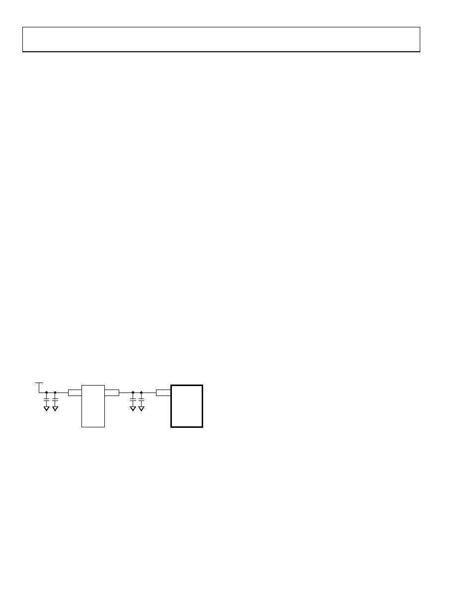
C40
100F
C39
0.1F
C35
0.1F
C34
10F
REFERENCE
SUPPLY
V+
VREF+
VOUT
VIN
06
85
9-
0
21
AD7767/
AD7767-1/
AD7767-2
ADR4xx
Figure 46. AD7767/AD7767-1/AD7767-2 Reference Input Configuration
MULTIPLEXING ANALOG INPUT CHANNELS
The AD7767/AD7767-1/AD7767-2 can be used with a multi-
plexer configuration. As per any converter that uses a digital
filtering block, the maximum switching rate or the output data
rate per channel is a function of the digital filter settling time.
A user multiplexing the analog inputs to a converter that
employs a digital filter must wait the full digital filter settling
time before a valid conversion result can be achieved; after this
settling time, the channel can be switched. Then, the full
settling time must again be observed before a valid conversion
result is available and the input is switched once more.
The AD7767 filter settling time equals 74 divided by the output
data rate in use. The maximum switching frequency in a
multiplexed application is, therefore, 1/(74/ODR), where the
output data rate (ODR) is a function of the applied MCLK
frequency and the decimation rate employed by the device in
question. For example, applying a 1.024 MHz MCLK frequency
to the AD7767 results in a maximum output data rate of 128 kHz,
which in turn allows a 1.729 kHz multiplexer switching rate.
The AD7767-1 and the AD7767-2 employ digital filters with
longer settling time to achieve greater precision; thus, the
maximum switching frequency for these devices is 864 Hz and
432 Hz, respectively.
相关PDF资料 |
PDF描述 |
|---|---|
| AD7776ARZ | IC ADC 10BIT 1CHAN HS 24SOIC |
| AD7780BRZ-REEL | IC ADC 24BIT 1CH LP SD 14SOIC |
| AD7781CRZ | IC ADC 20BIT 1CH LP SD 14SOIC |
| AD7782BRUZ | IC ADC 24BIT 2CHAN 16TSSOP |
| AD7783BRU | IC ADC 24BIT 2CH R-R 16-TSSOP |
相关代理商/技术参数 |
参数描述 |
|---|---|
| AD7768-4BSTZ | 功能描述:24 Bit Analog to Digital Converter 4 Input 4 Sigma-Delta 64-LQFP (10x10) 制造商:analog devices inc. 系列:- 包装:托盘 零件状态:有效 位数:24 采样率(每秒):256k 输入数:4 输入类型:差分 数据接口:SPI 配置:ADC 无线电 - S/H:ADC:- A/D 转换器数:4 架构:三角积分 参考类型:外部 电压 - 电源,模拟:2 V ~ 5.5 V 电压 - 电源,数字:- 特性:同步采样 工作温度:-40°C ~ 150°C 封装/外壳:64-LQFP 供应商器件封装:64-LQFP(10x10) 标准包装:1 |
| AD7768-4BSTZ-RL | 功能描述:24 Bit Analog to Digital Converter 4 Input 4 Sigma-Delta 64-LQFP (10x10) 制造商:analog devices inc. 系列:- 包装:带卷(TR) 零件状态:有效 位数:24 采样率(每秒):256k 输入数:4 输入类型:差分 数据接口:SPI 配置:ADC 无线电 - S/H:ADC:- A/D 转换器数:4 架构:三角积分 参考类型:外部 电压 - 电源,模拟:2 V ~ 5.5 V 电压 - 电源,数字:- 特性:同步采样 工作温度:-40°C ~ 150°C 封装/外壳:64-LQFP 供应商器件封装:64-LQFP(10x10) 标准包装:1,500 |
| AD7768-4BSTZ-RL7 | 功能描述:24 Bit Analog to Digital Converter 4 Input 4 Sigma-Delta 64-LQFP (10x10) 制造商:analog devices inc. 系列:- 包装:带卷(TR) 零件状态:有效 位数:24 采样率(每秒):256k 输入数:4 输入类型:差分 数据接口:SPI 配置:ADC 无线电 - S/H:ADC:- A/D 转换器数:4 架构:三角积分 参考类型:外部 电压 - 电源,模拟:2 V ~ 5.5 V 电压 - 电源,数字:- 特性:同步采样 工作温度:-40°C ~ 150°C 封装/外壳:64-LQFP 供应商器件封装:64-LQFP(10x10) 标准包装:500 |
| AD7768BSTZ | 功能描述:24 Bit Analog to Digital Converter 8 Input 8 Sigma-Delta 64-LQFP (10x10) 制造商:analog devices inc. 系列:- 包装:托盘 零件状态:有效 位数:24 采样率(每秒):256k 输入数:8 输入类型:差分,个伪差分 数据接口:SPI,DSP 配置:ADC 无线电 - S/H:ADC:- A/D 转换器数:8 架构:三角积分 参考类型:外部 电压 - 电源,模拟:2 V ~ 5.5 V 电压 - 电源,数字:2 V ~ 3.6 V 特性:同步采样 工作温度:-40°C ~ 105°C 封装/外壳:64-LQFP 供应商器件封装:64-LQFP(10x10) 标准包装:1 |
| AD7768BSTZ-RL | 功能描述:24 Bit Analog to Digital Converter 8 Input 8 Sigma-Delta 64-LQFP (10x10) 制造商:analog devices inc. 系列:- 包装:带卷(TR) 零件状态:有效 位数:24 采样率(每秒):256k 输入数:8 输入类型:差分,个伪差分 数据接口:SPI,DSP 配置:ADC 无线电 - S/H:ADC:- A/D 转换器数:8 架构:三角积分 参考类型:外部 电压 - 电源,模拟:2 V ~ 5.5 V 电压 - 电源,数字:2 V ~ 3.6 V 特性:同步采样 工作温度:-40°C ~ 105°C 封装/外壳:64-LQFP 供应商器件封装:64-LQFP(10x10) 标准包装:1,500 |
发布紧急采购,3分钟左右您将得到回复。