- 您现在的位置:买卖IC网 > PDF目录10210 > AD7777ARZ-REEL (Analog Devices Inc)IC ADC 10BIT 4CHAN HS 28SOIC PDF资料下载
参数资料
| 型号: | AD7777ARZ-REEL |
| 厂商: | Analog Devices Inc |
| 文件页数: | 6/12页 |
| 文件大小: | 0K |
| 描述: | IC ADC 10BIT 4CHAN HS 28SOIC |
| 标准包装: | 1,000 |
| 位数: | 10 |
| 采样率(每秒): | 378k |
| 数据接口: | 并联 |
| 转换器数目: | 1 |
| 电压电源: | 单电源 |
| 工作温度: | -40°C ~ 85°C |
| 安装类型: | 表面贴装 |
| 封装/外壳: | 28-SOIC(0.295",7.50mm 宽) |
| 供应商设备封装: | 28-SOIC W |
| 包装: | 带卷 (TR) |
| 输入数目和类型: | 4 个单端,单极 |
AD7776/AD7777/AD7778
–3–
REV. A
TIMING SPECIFICATIONS1, 2(V
CC = +5 V
5%; AGND = DGND = 0 V; all specifications TMIN to TMAX, unless otherwise noted.)
t
3
t
11
t
10
t
9
t
8
FIRST
CONVERSION
FINISHED
(CR6 = 0)
SECOND
CONVERSION
FINISHED (CR6 = 1)
AD7777/AD7778 ONLY
t
9
BUSY
(CR8 = 0)
INT
(CR8 = 1)
t
10
WR, RD
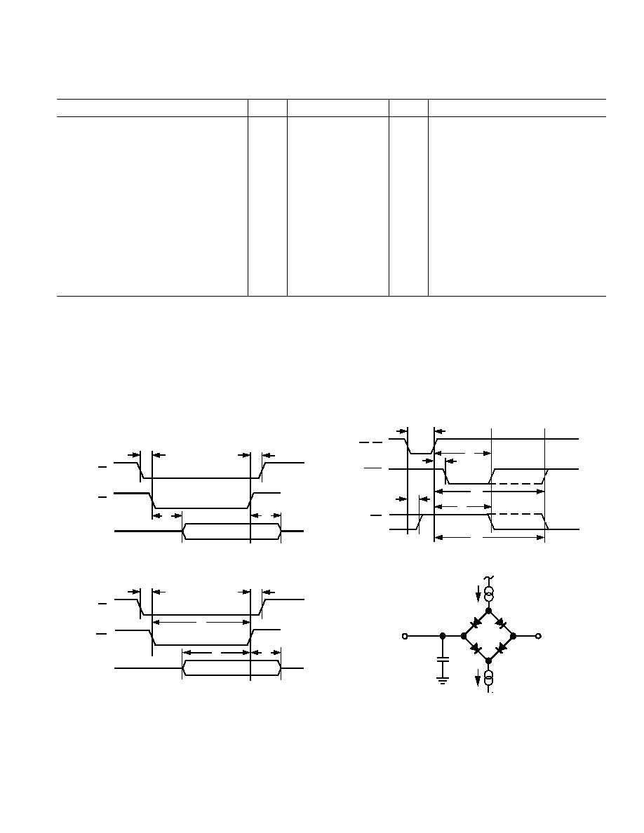
Figure 3.
BUSY/INT Timing
IOL
1.6mA
+2.1V
IOH
200
A
COUT
100pF
DB n
Figure 4. Load Circuit for Bus Timing Characteristics
t1
CS
t2
t4
t5
RD
DB0–DB9
Figure 1. Read Cycle Timing
t1
CS
t2
t6
WR
DB0–DB9
t3
t7
Figure 2. Write Cycle Timing
Parameter
Label
Limit at TMIN to TMAX Unit
Test Conditions/Comments
INTERFACE TIMING
CS Falling Edge to WR or RD Falling Edge
t1
0
ns min
WR or RD Rising Edge to CS Rising Edge
t2
0
ns min
WR Pulsewidth
t3
53
ns min
CS or RD Active to Valid Data3, 4
t4
60
ns max
Timed from Whichever Occurs Last
Bus Relinquish Time after
RD3, 5
t5
10
ns min
45
ns max
Data Valid to
WR Rising Edge
t6
55
ns min
Data Valid after
WR Rising Edge
t7
10
ns min
WR Rising Edge to BUSY Falling Edge
t8
1.5 tCLKIN
ns min
CR9 = 0
2.5 tCLKIN + 70
ns max
WR Rising Edge to BUSY Rising Edge or
INT Falling Edge
t9
19.5 tCLKIN + 70
ns max
Single Conversion, CR6 = 0
t10
33.5 tCLKIN + 70
ns max
Double Conversion, CR6 = 1
WR or RD Falling Edge to INT Rising Edge
t11
60
ns max
CR9 = 1
NOTES
1See Figures 1 to 3.
2All input signals are specified with tr = tf = 5 ns (10% to 90% of 5 V) and timed from a voltage level of 1.6 V.
3100% production tested. All other times are guaranteed by design, not production tested.
4t
4 is measured with the load circuit of Figure 4 and defined as the time required for an output to cross 0.8 V or 2.4 V.
5t
5 is derived from the measured time taken by the data outputs to change 0.5 V when loaded with the circuit of Figure 4. The measured time is then extrapolated back
to remove the effects of charging or discharging the 100 pF capacitor. This means that the time t 5 quoted above is the true bus relinquish time of the device and, as
such, is independent of the external bus loading capacitance.
Specifications subject to change without notice.
相关PDF资料 |
PDF描述 |
|---|---|
| VI-2NP-CU-F2 | CONVERTER MOD DC/DC 13.8V 200W |
| VE-2WX-MY | CONVERTER MOD DC/DC 5.2V 50W |
| VE-2WW-MY | CONVERTER MOD DC/DC 5.5V 50W |
| VE-2W0-MY | CONVERTER MOD DC/DC 5V 50W |
| MS3126F14-5PX | CONN PLUG 5POS STRAIGHT W/PINS |
相关代理商/技术参数 |
参数描述 |
|---|---|
| AD7778 | 制造商:AD 制造商全称:Analog Devices 功能描述:LC2MOS, High Speed 1-, 4- & 8-Channel 10-Bit ADCs |
| AD7778AS | 制造商:Analog Devices 功能描述:ADC Single SAR 378ksps 10-bit Parallel 44-Pin MQFP 制造商:Rochester Electronics LLC 功能描述:8-CH 10-BIT ADC IC - Bulk |
| AD7778ASZ | 功能描述:IC ADC 10BIT 8CHAN HS 44-MQFP RoHS:是 类别:集成电路 (IC) >> 数据采集 - 模数转换器 系列:- 标准包装:1 系列:- 位数:14 采样率(每秒):83k 数据接口:串行,并联 转换器数目:1 功率耗散(最大):95mW 电压电源:双 ± 工作温度:0°C ~ 70°C 安装类型:通孔 封装/外壳:28-DIP(0.600",15.24mm) 供应商设备封装:28-PDIP 包装:管件 输入数目和类型:1 个单端,双极 |
| AD7779ACPZ | 功能描述:24 Bit Analog to Digital Converter 8 Input 8 Sigma-Delta 64-LFCSP (9x9) 制造商:analog devices inc. 系列:- 包装:托盘 零件状态:有效 位数:24 采样率(每秒):16k 输入数:8 输入类型:差分,单端 数据接口:串行 配置:PGA-ADC 无线电 - S/H:ADC:- A/D 转换器数:8 架构:三角积分 参考类型:外部, 内部 电压 - 电源,模拟:±1.65V,2.2 V ~ 3.6 V 电压 - 电源,数字:- 特性:同步采样 工作温度:-40°C ~ 125°C 封装/外壳:64-WFQFN 裸露焊盘 供应商器件封装:64-LFCSP(9x9) 标准包装:1 |
发布紧急采购,3分钟左右您将得到回复。