- 您现在的位置:买卖IC网 > PDF目录10210 > AD7777ARZ-REEL (Analog Devices Inc)IC ADC 10BIT 4CHAN HS 28SOIC PDF资料下载
参数资料
| 型号: | AD7777ARZ-REEL |
| 厂商: | Analog Devices Inc |
| 文件页数: | 8/12页 |
| 文件大小: | 0K |
| 描述: | IC ADC 10BIT 4CHAN HS 28SOIC |
| 标准包装: | 1,000 |
| 位数: | 10 |
| 采样率(每秒): | 378k |
| 数据接口: | 并联 |
| 转换器数目: | 1 |
| 电压电源: | 单电源 |
| 工作温度: | -40°C ~ 85°C |
| 安装类型: | 表面贴装 |
| 封装/外壳: | 28-SOIC(0.295",7.50mm 宽) |
| 供应商设备封装: | 28-SOIC W |
| 包装: | 带卷 (TR) |
| 输入数目和类型: | 4 个单端,单极 |
AD7776/AD7777/AD7778
–5–
REV. A
PIN FUNCTION DESCRIPTION
Mnemonic
Description
VCC
+5 V Power Supply.
AGND
Analog Ground.
DGND
Digital Ground. Ground reference for digital circuitry.
DB0–DB9
Input/Output Data Bus. This is a bidirectional data port from which ADC output data may be read and to which
control register data may be written.
BUSY/INT
Busy/Interrupt Output. Active low logic output indicating A/D converter status. This logic output has two modes
of operation depending on whether location CR9 of the control register has been set low or high:
If CR9 is set low, the
BUSY/INT output behaves as a BUSY signal. The BUSY signal goes low and stays low for the
duration of a single conversion, or if simultaneous sampling has been selected,
BUSY stays low for the duration of
both conversions.
If CR9 is set high,
BUSY/INT output behaves as an INTERRUPT signal. The INT signal goes low and remains low
after either a single conversion is completed or after a double conversion is completed if simultaneous sampling has
been selected. With CR9 high, the falling edge of
WR or RD resets the INT line high.
CS
Chip Select Input. The device is selected when this input is low.
WR
Write Input (Active Low). It is used in conjunction with
CS to write data to the control register. Data is latched to the
registers on the rising edge of
WR. Following the rising edge of WR, the analog input is acquired and a conversion is
started.
RD
Read Input (Active Low). It is used in conjunction with
CS to enable the data outputs from the ADC registers.
AIN1–8
Analog Inputs 1–8. The analog input range is VBIAS
± V
SWING where VBIAS and VSWING are defined by the reference
voltage applied to REFIN. Input resistance between any of the analog input pins and AGND is 10 k
or greater.
REFIN
Voltage Reference Input. The AD7776/AD7777/AD7778 are specified over a voltage reference range of 1.9 V to 2.1 V
with a nominal value of 2.0 V. This REFIN voltage provides the VBIAS and VSWING levels for the input channel(s).
VBIAS is equal to REFIN and VSWING is nominally equal to REFIN/2. Input resistance between this REFIN pin and
AGND is 10 k
or greater.
REFOUT
Voltage Reference Output. This pin provides the internal voltage reference, which is nominally 2.0 V. It can provide
the bias voltage (VBIAS) for the input channel(s).
CREFIN
Reference Decoupling Capacitor. A 10 nF capacitor must be connected from this pin to AGND to ensure correct
operation of the high speed ADC.
RTN
Signal Return Path for the input channel(s). Normally RTN is connected to AGND at the package.
CIRCUIT DESCRIPTION
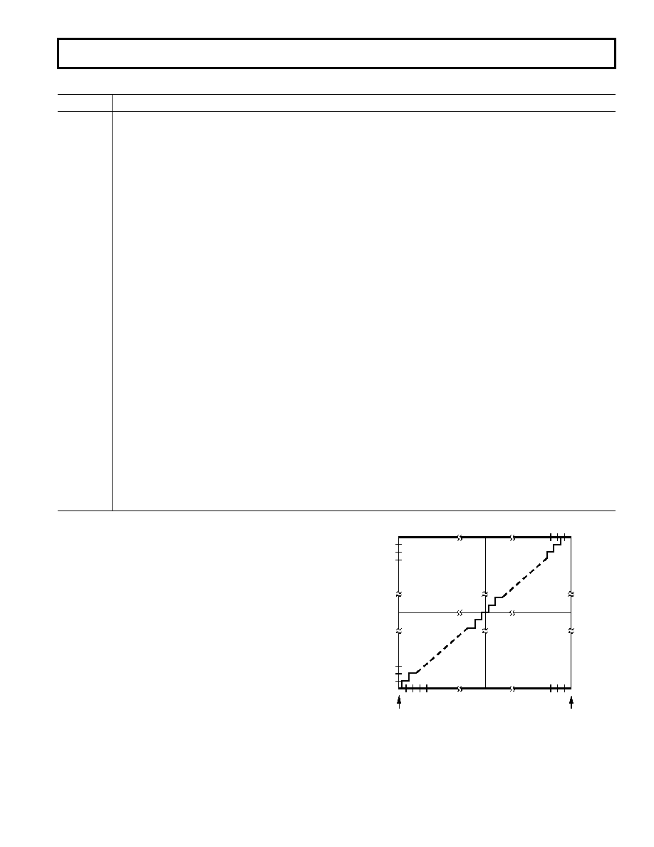
ADC Transfer Function
For all versions, an input signal of the form VBIAS
± VSWING is
expected. This VBIAS signal level operates as a pseudo ground to
which all input signals must be referred. The VBIAS level is
determined by the voltage applied to the REFIN pin. This can
be driven by an external voltage source or, alternatively, by the
onboard 2 V reference, available at REFOUT. The magnitude
of the input signal swing is equal to VBIAS/2 (or REFIN/2) and is
set internally. With a REFIN of 2 V, the analog input signal level
varies from 1 V to 3 V, i.e., 2
± 1 V. Figure 5 shows the transfer
function of the ADC and its relationship to VBIAS and VSWING.
The half-scale two's complement code of the ADC, 000 Hex (00
0000 0000 Binary), occurs at an input voltage equal to VBIAS. The
input full-scale range of the ADC is equal to 2 VSWING, so that the
Plus Full-Scale transition (1FE to 1FF) occurs at a voltage equal to
VBIAS + VSWING – 1.5 LSBs, and the minus full-scale code transi-
tion (200 to 201) occurs at a voltage VBIAS – VSWING + 0.5 LSBs.
ADC
OUTPUT
CODE
(HEX)
1FF
1FE
202
201
200
000
VBIAS–VSWING
VBIAS
VBIAS+VSWING
ANALOG INPUT, VIN
Figure 5. ADC Transfer Function
相关PDF资料 |
PDF描述 |
|---|---|
| VI-2NP-CU-F2 | CONVERTER MOD DC/DC 13.8V 200W |
| VE-2WX-MY | CONVERTER MOD DC/DC 5.2V 50W |
| VE-2WW-MY | CONVERTER MOD DC/DC 5.5V 50W |
| VE-2W0-MY | CONVERTER MOD DC/DC 5V 50W |
| MS3126F14-5PX | CONN PLUG 5POS STRAIGHT W/PINS |
相关代理商/技术参数 |
参数描述 |
|---|---|
| AD7778 | 制造商:AD 制造商全称:Analog Devices 功能描述:LC2MOS, High Speed 1-, 4- & 8-Channel 10-Bit ADCs |
| AD7778AS | 制造商:Analog Devices 功能描述:ADC Single SAR 378ksps 10-bit Parallel 44-Pin MQFP 制造商:Rochester Electronics LLC 功能描述:8-CH 10-BIT ADC IC - Bulk |
| AD7778ASZ | 功能描述:IC ADC 10BIT 8CHAN HS 44-MQFP RoHS:是 类别:集成电路 (IC) >> 数据采集 - 模数转换器 系列:- 标准包装:1 系列:- 位数:14 采样率(每秒):83k 数据接口:串行,并联 转换器数目:1 功率耗散(最大):95mW 电压电源:双 ± 工作温度:0°C ~ 70°C 安装类型:通孔 封装/外壳:28-DIP(0.600",15.24mm) 供应商设备封装:28-PDIP 包装:管件 输入数目和类型:1 个单端,双极 |
| AD7779ACPZ | 功能描述:24 Bit Analog to Digital Converter 8 Input 8 Sigma-Delta 64-LFCSP (9x9) 制造商:analog devices inc. 系列:- 包装:托盘 零件状态:有效 位数:24 采样率(每秒):16k 输入数:8 输入类型:差分,单端 数据接口:串行 配置:PGA-ADC 无线电 - S/H:ADC:- A/D 转换器数:8 架构:三角积分 参考类型:外部, 内部 电压 - 电源,模拟:±1.65V,2.2 V ~ 3.6 V 电压 - 电源,数字:- 特性:同步采样 工作温度:-40°C ~ 125°C 封装/外壳:64-WFQFN 裸露焊盘 供应商器件封装:64-LFCSP(9x9) 标准包装:1 |
发布紧急采购,3分钟左右您将得到回复。