参数资料
| 型号: | AD7804BRZ-REEL |
| 厂商: | Analog Devices Inc |
| 文件页数: | 15/28页 |
| 文件大小: | 0K |
| 描述: | IC DAC 10BIT QUAD SRL 16-SOIC |
| 产品培训模块: | Data Converter Fundamentals DAC Architectures |
| 标准包装: | 1,000 |
| 设置时间: | 1.5µs |
| 位数: | 10 |
| 数据接口: | 串行 |
| 转换器数目: | 4 |
| 电压电源: | 模拟和数字 |
| 功率耗散(最大): | 66mW |
| 工作温度: | -40°C ~ 85°C |
| 安装类型: | 表面贴装 |
| 封装/外壳: | 16-SOIC(0.295",7.50mm 宽) |
| 供应商设备封装: | 16-SOIC W |
| 包装: | 带卷 (TR) |
| 输出数目和类型: | 8 电压,双极 |
| 采样率(每秒): | 667k |
第1页第2页第3页第4页第5页第6页第7页第8页第9页第10页第11页第12页第13页第14页当前第15页第16页第17页第18页第19页第20页第21页第22页第23页第24页第25页第26页第27页第28页
AD7804/AD7805/AD7808/AD7809
REV. A
–22–
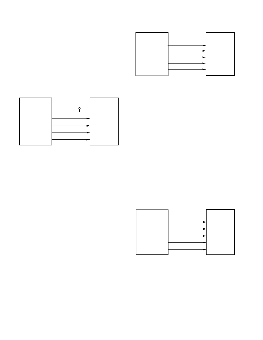
MICROPROCESSOR INTERFACING
AD7804/AD7808–ADSP-2101/ADSP-2103 Interface
Figure 35 shows a serial interface between the AD7804/AD7808
and the ADSP-2101/ADSP-2103. The ADSP-2101/ADSP-
2103 should be set up to operate in the SPORT Transmit Alter-
nate Framing Mode. The ADSP-2101/ADSP-2103 SPORT is
programmed through the SPORT control register and should be
configured as follows: Internal Clock Operation, Active Low
Framing, 16-bit Word Length. Transmission is initiated by
writing a word to the TX register after the SPORT has been
enabled. The data is clocked out on each rising edge of the serial
clock and clocked into the AD7804/AD7808 on the falling edge
of the SCLK.
+5V
LDAC
ADSP-2101/
ADSP-2103*
CLKIN
DT
*ADDITIONAL PINS OMITTED FOR CLARITY
FSIN
SDIN
SCLK
AD7804*/
AD7808
TFS
FO
CLR
Figure 35. ADSP-2101/ADSP-2103 Interface
AD7804/AD7808–68HC11/68L11 Interface
Figure 36 shows a serial interface between the AD7804/AD7808
and the 68HC11/68L11 microcontroller. SCK of the 68HC11/
68L11 drives the CLKIN of the AD7804/AD7808, while the
MOSI output drives the serial data line of the DAC. The
FSIN
signal is derived from a port line (PC7). The setup conditions
for correct operation of this interface are as follows: the
68HC11/68L11 should be configured so that its CPOL bit is a 0
and its CPHA bit is a 1. When data is being transmitted to the
DAC the
FSIN line is taken low (PC7). When the 68HC11/
68L11 is configured as above, data appearing on the MOSI
output is valid on the falling edge of SCK. Serial data from the
68HC11/68L11 is transmitted in 8-bit bytes with only eight
falling clock edges occurring in the transmit cycle. Data is trans-
mitted MSB first. In order to load data to the AD7804/AD7808,
PC7 is left low after the first eight bits are transferred and a
second serial write operation is performed to the DAC and then
PC7 is taken high at the end of this procedure. In the diagram
shown
LDAC and CLR are also controlled from the bit pro-
grammable lines of the 68HC11/68L11. The user can bring
LDAC low after every two bytes have been transmitted to up-
date that particular DAC which has been programmed or alter-
natively it is possible to wait until all the input registers have
been loaded before updating takes place.
LDAC
68HC11/68L11*
SDIN
SCK
*ADDITIONAL PINS OMITTED FOR CLARITY
FSIN
CLKIN
MOSI
AD7804*/
AD7808
PC7
PC6
PC5
CLR
Figure 36. AD7804/AD7808–68HC11/68L11 Interface
AD7804/AD7808–80C51/80L51 Interface
Figure 37 shows a serial interface between the AD7804/AD7808
and the 80C51/80L51 microcontroller. The setup for the inter-
face is as follows, TXD of the 80C51/80L51 drives CLKIN of
the AD7804/AD7808 while RXD drives the serial data line of
the part. The
FSIN signal is again derived from a bit program-
mable pin on the port in this case port line P3.3 is used. When
data is to be transmitted to the part, P3.3 is taken low. Data on
RXD is valid on the falling edge of TXD. The 80C51/80L51
transmits data in eight bit bytes thus only eight falling clock
edges occur in the transmit cycle. To load data to the DAC,
P3.3 is left low after the first eight bits are transmitted and a
second write cycle is initiated to transmit the second byte of
data, P3.3 is taken high following the completion of this cycle.
The 80C51/80L51 outputs the serial data in a format which has
the LSB first. The AD7804/AD7808 requires its data with the
MSB as the first bit received. The 80C51/80L51 transmit rou-
tine should take this into account. In the diagram shown
LDAC
and
CLR are also controlled from the bit programmable lines of
the 80C51/80L51 port. The user can bring
LDAC low after
every two bytes have been transmitted to update that particular
DAC which has been programmed or alternatively it is possible
to wait until all the input registers have been loaded before
updating takes place.
LDAC
80C51/80L51*
SDIN
TXD
*ADDITIONAL PINS OMITTED FOR CLARITY
FSIN
SCLK
RXD
AD7804*/
AD7808
P3.4
P3.5
P3.3
CLR
Figure 37. AD7804/AD7808–80C51/80L51 Interface
相关PDF资料 |
PDF描述 |
|---|---|
| AD5328ARUZ-REEL7 | IC DAC 12BIT OCTAL W/BUF 16TSSOP |
| AD5325BRMZ-REEL7 | IC DAC 12BIT 2WIRE I2C 10MSOP |
| AD5325BRMZ-REEL | IC DAC 12BIT 2WIRE I2C 10MSOP |
| AD5531BRUZ-REEL7 | IC DAC 14BIT SRL IN/VOUT 16TSSOP |
| AD5531BRUZ-REEL | IC DAC 14BIT SRL IN/VOUT 16TSSOP |
相关代理商/技术参数 |
参数描述 |
|---|---|
| AD7804CN | 制造商:未知厂家 制造商全称:未知厂家 功能描述:10-Bit Digital-to-Analog Converter |
| AD7804CR | 制造商:未知厂家 制造商全称:未知厂家 功能描述:10-Bit Digital-to-Analog Converter |
| AD7805 | 制造商:AD 制造商全称:Analog Devices 功能描述:+3.3 V to +5 V Quad/Octal 10-Bit DACs |
| AD7805BN | 制造商:Analog Devices 功能描述:DAC 4-CH 10-bit 28-Pin PDIP W Tube 制造商:Rochester Electronics LLC 功能描述:QUAD 10-BIT PARALLEL DAC - Bulk |
| AD7805BNZ | 功能描述:IC DAC 10BIT QUAD PARALLEL 28DIP RoHS:是 类别:集成电路 (IC) >> 数据采集 - 数模转换器 系列:- 产品培训模块:Data Converter Fundamentals DAC Architectures 标准包装:750 系列:- 设置时间:7µs 位数:16 数据接口:并联 转换器数目:1 电压电源:双 ± 功率耗散(最大):100mW 工作温度:0°C ~ 70°C 安装类型:表面贴装 封装/外壳:28-LCC(J 形引线) 供应商设备封装:28-PLCC(11.51x11.51) 包装:带卷 (TR) 输出数目和类型:1 电压,单极;1 电压,双极 采样率(每秒):143k |
发布紧急采购,3分钟左右您将得到回复。