参数资料
| 型号: | AD7804BRZ-REEL |
| 厂商: | Analog Devices Inc |
| 文件页数: | 2/28页 |
| 文件大小: | 0K |
| 描述: | IC DAC 10BIT QUAD SRL 16-SOIC |
| 产品培训模块: | Data Converter Fundamentals DAC Architectures |
| 标准包装: | 1,000 |
| 设置时间: | 1.5µs |
| 位数: | 10 |
| 数据接口: | 串行 |
| 转换器数目: | 4 |
| 电压电源: | 模拟和数字 |
| 功率耗散(最大): | 66mW |
| 工作温度: | -40°C ~ 85°C |
| 安装类型: | 表面贴装 |
| 封装/外壳: | 16-SOIC(0.295",7.50mm 宽) |
| 供应商设备封装: | 16-SOIC W |
| 包装: | 带卷 (TR) |
| 输出数目和类型: | 8 电压,双极 |
| 采样率(每秒): | 667k |
第1页当前第2页第3页第4页第5页第6页第7页第8页第9页第10页第11页第12页第13页第14页第15页第16页第17页第18页第19页第20页第21页第22页第23页第24页第25页第26页第27页第28页
AD7804/AD7805/AD7808/AD7809
REV. A
–10–
DB15 (MSB)
DB0 (LSB)
X
MD0 = 1
MD1 = 0
A2*
A1
A0
MX1
MX0
X
STBY
CLR
0
X
X = Don’t Care
*Applicable to the AD7808 Only, and Are Don’t Care Conditions when Operating the AD7804 .
Figure 5. AD7804/AD7808 Channel Control Register Loading Sequence
DB15 (MSB)
DB0 (LSB)
MAIN/SUB
MD0 = X
MD1 = 1 A2* A1
A0
DB9 DB8
DB7
DB6 DB5 DB4
DB3 DB2
DB1 DB0
X = Don’t Care
*Applicable to the AD7808 Only, and Are Don’t Care Conditions when Operating the AD7804 .
Figure 6. AD7804/AD7808 Main DAC Data Register Loading Sequence (
MAIN/SUB = 0)
DB15 (MSB)
DB0 (LSB)
MAIN/SUB
MD0 = X
MD1 = 1 A2* A1
A0
DB7 DB6
DB5
DB4 DB3 DB2
DB1 DB0
X
X = Don’t Care
*Applicable to the AD7808 Only, and Are Don’t Care Conditions when Operating the AD7804.
Figure 7. AD7804/AD7808 Sub DAC Data Register Loading Sequence (
MAIN/SUB = 1)
MSB
LSB
X
MD0 = 0
MD1 = 0
X
XXXX0
BIN/
COMP
PD SSTBY
SCLR
0
X
X = Don’t Care
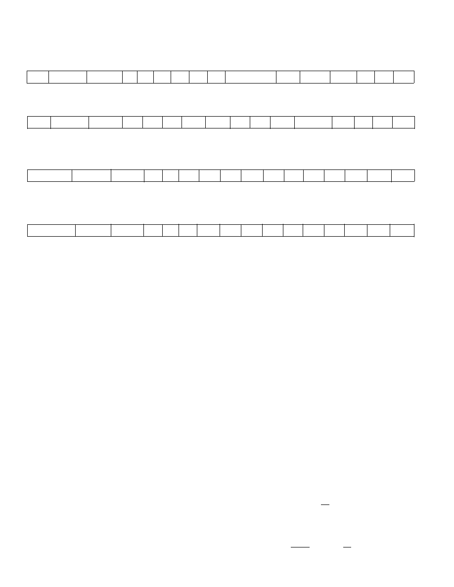
Figure 4. AD7804/AD7808 System Control Register Loading Sequence
AD7804/AD7808 SYSTEM CONTROL REGISTER (MD1 = 0,
MD0 = 0)
The bits in this register allow control over all DACs in the
package. The control bits include power down (
PD), DAC input
coding select (BIN/
COMP), system standby (SSTBY) and a
system clear (SCLR). The function of these bits is as follows:
Power Down
(PD)
This bit in the control register is used to shut down the complete
device. With a 0 in this position, the reference and all DACs are
put into low power mode. Writing a 1 to this bit puts the part in
the normal operating mode. When in power-down mode, the
contents of all registers are retained and are valid when the
device is put back into normal operation.
Coding (BIN/
COMP)
This bit in the system control register allows the user to select
one of two input coding schemes. The available schemes are
Twos complement coding and offset binary coding. All DACs
will be configured with the same input coding scheme. Writing
a zero to the control register selects twos complement coding,
while writing a 1 to this bit in the control register selects offset
binary coding.
With twos complement coding selected the output voltage from
the Main DAC is of the form :
V
OUT = VBIAS ± VSWING
where
VSWING is
15
16
×V
BIAS
With Offset Binary coding selected the output voltage from the
Main DAC ranges from:
VOUT =
VBIAS
16
to VOUT =
31
16
× VBIAS
When the system control register is selected by writing zeros to
the mode bits, MD1 and MD0 the address bits are ignored as
the system control register controls all DACs in the package.
When MD1 = 0 and MD0 = 1, writing is to the channel control
register. Only the DAC selected by the address bits will be af-
fected by writing to this register. Each individual DAC has a
channel control register.
The DACs data registers are addressed by writing a one to
MD1 (DB13); the condition of MD0 (DB14) does not matter
when writing to the data registers. DB15 determines whether
writing is to the Main DAC data register or to the Sub DAC
data register. The Main DAC is 10 bits wide and the Sub DAC
is 8 bits wide. Thus when writing to the Sub DAC DB1 and
DB0 become don’t cares. The Sub DAC is used to offset the
complete transfer function of the Main DAC around its VBIAS
point. The Sub DAC has 1/8 LSB resolution and will enable the
transfer function of the Main DAC to be offset by
± V
BIAS/32.
When the
LDAC line goes low, all DAC registers in the device
are simultaneously loaded with the contents of their respective
DAC data registers, and the outputs change accordingly.
Bringing the
CLR line low resets the DAC data and DAC regis-
ters. This hardware clear affects both the Main and Sub DACs.
This operation sets the analog output of the Main DAC to VBIAS/
16 when offset binary coding is selected and the output is set to
VBIAS when twos complement coding is used. VBIAS is the output
of the internal multiplexer as shown in Figure 3. The output of
the Sub DAC is used to shift the transfer function of the Main
DAC around the VBIAS point and the contribution from the Sub
DAC is zero following an external hardware clear. Software
clears affect the Main DACs only.
相关PDF资料 |
PDF描述 |
|---|---|
| AD5328ARUZ-REEL7 | IC DAC 12BIT OCTAL W/BUF 16TSSOP |
| AD5325BRMZ-REEL7 | IC DAC 12BIT 2WIRE I2C 10MSOP |
| AD5325BRMZ-REEL | IC DAC 12BIT 2WIRE I2C 10MSOP |
| AD5531BRUZ-REEL7 | IC DAC 14BIT SRL IN/VOUT 16TSSOP |
| AD5531BRUZ-REEL | IC DAC 14BIT SRL IN/VOUT 16TSSOP |
相关代理商/技术参数 |
参数描述 |
|---|---|
| AD7804CN | 制造商:未知厂家 制造商全称:未知厂家 功能描述:10-Bit Digital-to-Analog Converter |
| AD7804CR | 制造商:未知厂家 制造商全称:未知厂家 功能描述:10-Bit Digital-to-Analog Converter |
| AD7805 | 制造商:AD 制造商全称:Analog Devices 功能描述:+3.3 V to +5 V Quad/Octal 10-Bit DACs |
| AD7805BN | 制造商:Analog Devices 功能描述:DAC 4-CH 10-bit 28-Pin PDIP W Tube 制造商:Rochester Electronics LLC 功能描述:QUAD 10-BIT PARALLEL DAC - Bulk |
| AD7805BNZ | 功能描述:IC DAC 10BIT QUAD PARALLEL 28DIP RoHS:是 类别:集成电路 (IC) >> 数据采集 - 数模转换器 系列:- 产品培训模块:Data Converter Fundamentals DAC Architectures 标准包装:750 系列:- 设置时间:7µs 位数:16 数据接口:并联 转换器数目:1 电压电源:双 ± 功率耗散(最大):100mW 工作温度:0°C ~ 70°C 安装类型:表面贴装 封装/外壳:28-LCC(J 形引线) 供应商设备封装:28-PLCC(11.51x11.51) 包装:带卷 (TR) 输出数目和类型:1 电压,单极;1 电压,双极 采样率(每秒):143k |
发布紧急采购,3分钟左右您将得到回复。