参数资料
| 型号: | AD7805BRSZ |
| 厂商: | Analog Devices Inc |
| 文件页数: | 4/28页 |
| 文件大小: | 0K |
| 描述: | IC DAC 10BIT QUAD PARALL 28-SSOP |
| 产品培训模块: | Data Converter Fundamentals DAC Architectures |
| 标准包装: | 47 |
| 设置时间: | 1.5µs |
| 位数: | 10 |
| 数据接口: | 并联 |
| 转换器数目: | 4 |
| 电压电源: | 模拟和数字 |
| 功率耗散(最大): | 66mW |
| 工作温度: | -40°C ~ 85°C |
| 安装类型: | 表面贴装 |
| 封装/外壳: | 28-SSOP(0.209",5.30mm 宽) |
| 供应商设备封装: | 28-SSOP |
| 包装: | 管件 |
| 输出数目和类型: | 8 电压,双极 |
| 采样率(每秒): | 667k |
第1页第2页第3页当前第4页第5页第6页第7页第8页第9页第10页第11页第12页第13页第14页第15页第16页第17页第18页第19页第20页第21页第22页第23页第24页第25页第26页第27页第28页
AD7804/AD7805/AD7808/AD7809
REV. A
–12–
determined by MX1 and MX0 in the channel control register as
shown in Table III. The internal VDD/2 reference is provided at
the COMP pin. This internal reference can be overdriven with
an external reference thus providing the facility for two external
references.
AD7804/AD7808 POWER-UP CONDITIONS
When power is applied to the device, the device will come up in
standby mode where all the linear circuitry excluding the refer-
ence are switched off. Figure 8 shows the relevant default val-
ues for the system control register. Since a write to the system
control register is required to remove the standby condition the
only bits for which default conditions are applicable are
PD and
SSTBY. Figure 9 details the relevant default conditions for the
Channel Control Register.
PD
SSTBY
11
Figure 8. Default Conditions for System Control Register
on Power-Up
STBY
CLR
MX1
MX0
1
0
Figure 9. Default Conditions for Channel Control Register
on Power-Up
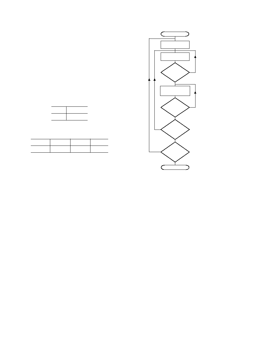
After power has been applied to the device the following proce-
dure should be followed to communicate and set up the device.
First, a write to the system control register is required to clear
the SSTBY bit and change the input coding scheme if required.
For example, to remove standby and set up offset binary input
coding 0060Hex should be written to the input register, if twos
complement coding is required 0020Hex should be written to
the input register. MD1 and MD0 are decoded in the input
register and this allows the data to be written to the system
control register.
Step two requires writing to the channel control register, which
allows individual control over each DAC in the package and
allows the VBIAS for the DAC to be selected as well as individual
DAC standby and clear functions. For example, if channel A is
to be configured for normal operation with internal reference
selected then 4110Hex should be written to the input register.
In the input register, the MD1 and MD0 bits are decoded in
association with the address bits to give access to the required
channel control register. The third and final step is to write data
to the selected DAC. To write half scale to channel A Main
DAC, 2200Hex should be written to the input register, the
MSB in the sixteen bit stream selects the Main DAC and the
next three bits address the DAC and the final 10 bits contain
the data. To write half scale to channel A Sub DAC, then A200
should be written to the input register. The flowchart in Figure
10 shows in graphic form the steps required in communicating
with the AD7804/AD7808.
WRITE TO SYSTEM
CONTROL REGISTER
WRITE TO CHANNEL
CONTROL REGISTER
SYSTEM
CONFIGURATION
CHANNEL
CONFIGURATION
DATA WRITE
N
Y
ALL CHANNELS
CONFIGURED
DATA LOADING
COMPLETE
WRITE TO SELECTED
MAIN OR SUB DAC
DATA REGISTERS
CHANGE
CHANNEL
CONFIGURATION
CHANGE
SYSTEM
CONFIGURATION
END
POWER-UP
Figure 10. Flowchart for Controlling the DAC Following
Power-Up
AD7805/AD7809 INTERFACE SECTION
The AD7805 and AD7809 are parallel data input devices and
contain both control registers and data registers. The system
control register has global control over all DACs in the package
while the channel control register allows control over individual
DACs in the package. Two data registers are also available, one
for the 10-bit Main DAC and the second for the 8-bit Sub
DAC. In the parallel mode,
CS and WR, in association with the
address pins, control the loading of data. Data is transferred
from the data register to the DAC register under the control of
the
LDAC signal. Only data contained in the DAC register deter-
mines the analog output of any DAC. The timing diagram for
10-bit parallel loading is shown in Figure 2. The MODE pin on
the device determines whether writing is to the data registers or
to the control registers. When MODE is at a logic one, writing
is to the data registers. In the next write to the data registers a
bit in the channel control register determines whether the Main
DAC or the Sub DAC is addressed. This means that to address
either the Main or the Sub DAC the
Main/Sub bit in the control
register has to be set appropriately before the data register write.
A logic zero on the mode pin enables writing to the control
register. Bit MD0 determines whether writing is to the system
control register or to the addressed channel control register.
Bringing the
CLR line low resets the DAC registers to one of
two known conditions depending on the coding scheme se-
lected. The hardware clear affects both the Main and Sub
DAC registers. With offset binary coding a clear sets the output
相关PDF资料 |
PDF描述 |
|---|---|
| VI-B7K-MY-F2 | CONVERTER MOD DC/DC 40V 50W |
| VI-JWB-MZ-F2 | CONVERTER MOD DC/DC 95V 25W |
| VI-B7J-MY-F3 | CONVERTER MOD DC/DC 36V 50W |
| VI-B7H-MY-F1 | CONVERTER MOD DC/DC 52V 50W |
| AD9115BCPZ | IC DAC DUAL 10BIT LO PWR 40LFCSP |
相关代理商/技术参数 |
参数描述 |
|---|---|
| AD7805BRSZ-REEL | 功能描述:IC DAC 10BIT QUAD PARALL 28-SSOP RoHS:是 类别:集成电路 (IC) >> 数据采集 - 数模转换器 系列:- 标准包装:47 系列:- 设置时间:2µs 位数:14 数据接口:并联 转换器数目:1 电压电源:单电源 功率耗散(最大):55µW 工作温度:-40°C ~ 85°C 安装类型:表面贴装 封装/外壳:28-SSOP(0.209",5.30mm 宽) 供应商设备封装:28-SSOP 包装:管件 输出数目和类型:1 电流,单极;1 电流,双极 采样率(每秒):* |
| AD7805BRSZ-REEL7 | 功能描述:IC DAC 10BIT QUAD PARALL 28SSOP RoHS:是 类别:集成电路 (IC) >> 数据采集 - 数模转换器 系列:- 标准包装:47 系列:- 设置时间:2µs 位数:14 数据接口:并联 转换器数目:1 电压电源:单电源 功率耗散(最大):55µW 工作温度:-40°C ~ 85°C 安装类型:表面贴装 封装/外壳:28-SSOP(0.209",5.30mm 宽) 供应商设备封装:28-SSOP 包装:管件 输出数目和类型:1 电流,单极;1 电流,双极 采样率(每秒):* |
| AD7805BRZ | 功能描述:IC DAC 10BIT QUAD PARALL 28-SOIC RoHS:是 类别:集成电路 (IC) >> 数据采集 - 数模转换器 系列:- 标准包装:1 系列:- 设置时间:4.5µs 位数:12 数据接口:串行,SPI? 转换器数目:1 电压电源:单电源 功率耗散(最大):- 工作温度:-40°C ~ 125°C 安装类型:表面贴装 封装/外壳:8-SOIC(0.154",3.90mm 宽) 供应商设备封装:8-SOICN 包装:剪切带 (CT) 输出数目和类型:1 电压,单极;1 电压,双极 采样率(每秒):* 其它名称:MCP4921T-E/SNCTMCP4921T-E/SNRCTMCP4921T-E/SNRCT-ND |
| AD7805BRZ-REEL | 功能描述:IC DAC 10BIT QUAD PARALL 28-SOIC RoHS:是 类别:集成电路 (IC) >> 数据采集 - 数模转换器 系列:- 标准包装:47 系列:- 设置时间:2µs 位数:14 数据接口:并联 转换器数目:1 电压电源:单电源 功率耗散(最大):55µW 工作温度:-40°C ~ 85°C 安装类型:表面贴装 封装/外壳:28-SSOP(0.209",5.30mm 宽) 供应商设备封装:28-SSOP 包装:管件 输出数目和类型:1 电流,单极;1 电流,双极 采样率(每秒):* |
| AD7805CN | 制造商:未知厂家 制造商全称:未知厂家 功能描述:10-Bit Digital-to-Analog Converter |
发布紧急采购,3分钟左右您将得到回复。