参数资料
| 型号: | AD7805BRSZ |
| 厂商: | Analog Devices Inc |
| 文件页数: | 5/28页 |
| 文件大小: | 0K |
| 描述: | IC DAC 10BIT QUAD PARALL 28-SSOP |
| 产品培训模块: | Data Converter Fundamentals DAC Architectures |
| 标准包装: | 47 |
| 设置时间: | 1.5µs |
| 位数: | 10 |
| 数据接口: | 并联 |
| 转换器数目: | 4 |
| 电压电源: | 模拟和数字 |
| 功率耗散(最大): | 66mW |
| 工作温度: | -40°C ~ 85°C |
| 安装类型: | 表面贴装 |
| 封装/外壳: | 28-SSOP(0.209",5.30mm 宽) |
| 供应商设备封装: | 28-SSOP |
| 包装: | 管件 |
| 输出数目和类型: | 8 电压,双极 |
| 采样率(每秒): | 667k |
第1页第2页第3页第4页当前第5页第6页第7页第8页第9页第10页第11页第12页第13页第14页第15页第16页第17页第18页第19页第20页第21页第22页第23页第24页第25页第26页第27页第28页
AD7804/AD7805/AD7808/AD7809
–13–
REV. A
DB9
DB0
DB9
DB8
DB7
DB6
DB5
DB4
DB3
DB2
DB1
DB0
DB7
DB6
DB5
DB4
DB3
DB2
DB1
DB0
X
X = Don’t Care
Figure 14. AD7805/AD7809 Main DAC Data Register (Top)
and Sub DAC Data Register (Bottom) Configuration
(MODE = 1,
10/8 = 0)
Figure 15 shows the bit allocations when 8-bit parallel operation
is selected in the system control register. DB9 to DB2 are re-
tained as data bits. DB1 acts as a high byte or low byte enable.
When DB1 is low, the eight MSBs of the data word are loaded
to the input register. When DB1 is high, the low byte consisting
of the two LSBs are loaded to the input register. DB0 is used to
select either the Main or Sub DAC when in the byte mode.
DB9
DB2
DB1
DB0
DB9 DB8 DB7 DB6 DB5 DB4 DB3 DB2
0
MAIN/SUB
X
XDB1 DB0
1
MAIN/SUB
X = Don’t Care
Figure 15. AD7805/AD7809 Main DAC Data Register Con-
figuration (MODE = 1,
10/8 = 1, MAIN/SUB = 0)
Figure 16 shows the bit allocations for writing to the Sub DAC.
DB9
DB2
DB1
DB0
DB7
DB6 DB5 DB4 DB3 DB2 DB1 DB0
X
MAIN/SUB
X = Don’t Care
Figure 16. AD7805/AD7809 Sub DAC Data Register Con-
figuration (MODE = 1,
MAIN/SUB = 1)
Each DAC has a separate channel control register. The follow-
ing is a brief discussion on the bits in each of the control registers.
DAC Selection (A2, A1, A0)
The external address pins in conjunction with
CS, WR and
MODE are used to address the various DAC data and control
registers. Table IVa shows how these DAC registers can be
addressed on the AD7805. Table IVb shows how these registers
are addressed on the AD7809. Refer to Figures 12 to 16 for infor-
mation on the registers.
Table IVa. AD7805 DAC Data/Control Register
Selection Table
MODE
A1
A0
Function Selected
0
DAC A Control Registers
0
1
DAC B Control Registers
0
1
0
DAC C Control Registers
0
1
DAC D Control Registers
1
0
DAC A Data Registers
1
0
1
DAC B Data Registers
1
0
DAC C Data Registers
1
DAC D Data Registers
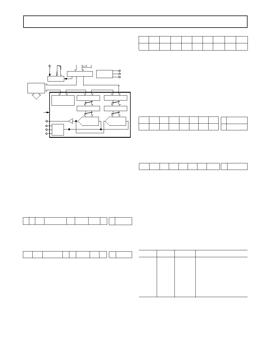
of the Main DAC to the bottom of the transfer function, VBIAS/16.
With twos complement coding the output of the DAC is cleared
to midscale which is VBIAS. A hardware clear always clears the
output of the Sub DAC to midscale thus the output of the Sub
DAC makes zero contribution to the output of the channel.
D9
D2 D1 D0
MODE ADDR
DATA REGISTER
8
VBIAS
INTERNAL VREF
VDD/2
REFIN
VOUT
CS
TO ALL
CHANNELS
SINGLE
CHANNEL
DAC REGISTER
8
8-BIT DAC
(SUB DAC)
DATA REGISTER
10
DAC REGISTER
10
10-BIT DAC
(MAIN DAC)
CHANNEL
CONTROL
REGISTER
MUX
SYSTEM
CONTROL
REGISTER
DECODER
CONTROL
LOGIC
WR
LDAC
INPUT REGISTER
Figure 11. AD7805/AD7809 Internal Registers
AD7805/AD7809 CONTROL REGISTERS
Access to the control registers of the AD7805/AD7809 is
achieved by taking the mode pin to a logic low. The control
register of these DACs are configured as in Figures 12 and 13.
There are two control registers associated with the part. System
control register which looks after the input coding, data format,
power down, system clear and system standby. The channel
control register contains bits that affect the operation of the
selected DAC. The external address bits are used to select the
DACs. These registers are eight bits wide and the last two bits
are control bits. The mode pin must be low to have access to the
control registers.
DB9
DB2 DB1
DB0
XX
10/8 BIN/COMP PD SSTBY SCLR 0
X
MD0 = 0
X = Don’t Care
Figure 12. AD7805/AD7809 System Control Register Con-
figuration, (MODE = 0)
DB9
DB2
DB1
DB0
MX1 MX0
MAIN/SUB X
X
STBY CLR 0
X
MD0 = 1
X = Don’t Care
Figure 13. AD7805/AD7809 Channel Control Register Con-
figuration (MODE = 0)
The external mode pin must be taken high to allow data to be
written to the DAC data registers. Figure 14 shows the bit allo-
cations when 10-bit parallel operation is selected in the system
control register.
相关PDF资料 |
PDF描述 |
|---|---|
| VI-B7K-MY-F2 | CONVERTER MOD DC/DC 40V 50W |
| VI-JWB-MZ-F2 | CONVERTER MOD DC/DC 95V 25W |
| VI-B7J-MY-F3 | CONVERTER MOD DC/DC 36V 50W |
| VI-B7H-MY-F1 | CONVERTER MOD DC/DC 52V 50W |
| AD9115BCPZ | IC DAC DUAL 10BIT LO PWR 40LFCSP |
相关代理商/技术参数 |
参数描述 |
|---|---|
| AD7805BRSZ-REEL | 功能描述:IC DAC 10BIT QUAD PARALL 28-SSOP RoHS:是 类别:集成电路 (IC) >> 数据采集 - 数模转换器 系列:- 标准包装:47 系列:- 设置时间:2µs 位数:14 数据接口:并联 转换器数目:1 电压电源:单电源 功率耗散(最大):55µW 工作温度:-40°C ~ 85°C 安装类型:表面贴装 封装/外壳:28-SSOP(0.209",5.30mm 宽) 供应商设备封装:28-SSOP 包装:管件 输出数目和类型:1 电流,单极;1 电流,双极 采样率(每秒):* |
| AD7805BRSZ-REEL7 | 功能描述:IC DAC 10BIT QUAD PARALL 28SSOP RoHS:是 类别:集成电路 (IC) >> 数据采集 - 数模转换器 系列:- 标准包装:47 系列:- 设置时间:2µs 位数:14 数据接口:并联 转换器数目:1 电压电源:单电源 功率耗散(最大):55µW 工作温度:-40°C ~ 85°C 安装类型:表面贴装 封装/外壳:28-SSOP(0.209",5.30mm 宽) 供应商设备封装:28-SSOP 包装:管件 输出数目和类型:1 电流,单极;1 电流,双极 采样率(每秒):* |
| AD7805BRZ | 功能描述:IC DAC 10BIT QUAD PARALL 28-SOIC RoHS:是 类别:集成电路 (IC) >> 数据采集 - 数模转换器 系列:- 标准包装:1 系列:- 设置时间:4.5µs 位数:12 数据接口:串行,SPI? 转换器数目:1 电压电源:单电源 功率耗散(最大):- 工作温度:-40°C ~ 125°C 安装类型:表面贴装 封装/外壳:8-SOIC(0.154",3.90mm 宽) 供应商设备封装:8-SOICN 包装:剪切带 (CT) 输出数目和类型:1 电压,单极;1 电压,双极 采样率(每秒):* 其它名称:MCP4921T-E/SNCTMCP4921T-E/SNRCTMCP4921T-E/SNRCT-ND |
| AD7805BRZ-REEL | 功能描述:IC DAC 10BIT QUAD PARALL 28-SOIC RoHS:是 类别:集成电路 (IC) >> 数据采集 - 数模转换器 系列:- 标准包装:47 系列:- 设置时间:2µs 位数:14 数据接口:并联 转换器数目:1 电压电源:单电源 功率耗散(最大):55µW 工作温度:-40°C ~ 85°C 安装类型:表面贴装 封装/外壳:28-SSOP(0.209",5.30mm 宽) 供应商设备封装:28-SSOP 包装:管件 输出数目和类型:1 电流,单极;1 电流,双极 采样率(每秒):* |
| AD7805CN | 制造商:未知厂家 制造商全称:未知厂家 功能描述:10-Bit Digital-to-Analog Converter |
发布紧急采购,3分钟左右您将得到回复。