参数资料
| 型号: | AD7808BRZ |
| 厂商: | Analog Devices Inc |
| 文件页数: | 10/28页 |
| 文件大小: | 0K |
| 描述: | IC DAC 10BIT OCTAL SRL 24-SOIC |
| 产品培训模块: | Data Converter Fundamentals DAC Architectures |
| 标准包装: | 31 |
| 设置时间: | 1.5µs |
| 位数: | 10 |
| 数据接口: | 串行 |
| 转换器数目: | 4 |
| 电压电源: | 模拟和数字 |
| 功率耗散(最大): | 99mW |
| 工作温度: | -40°C ~ 85°C |
| 安装类型: | 表面贴装 |
| 封装/外壳: | 24-SOIC(0.295",7.50mm 宽) |
| 供应商设备封装: | 24-SOIC W |
| 包装: | 管件 |
| 输出数目和类型: | 8 电压,双极 |
| 采样率(每秒): | 667k |
| 产品目录页面: | 785 (CN2011-ZH PDF) |
第1页第2页第3页第4页第5页第6页第7页第8页第9页当前第10页第11页第12页第13页第14页第15页第16页第17页第18页第19页第20页第21页第22页第23页第24页第25页第26页第27页第28页
AD7804/AD7805/AD7808/AD7809
REV. A
–18–
OFFSET BINARY CODING
Table VIII shows the offset binary transfer function for the Main
DAC.
Table VIII. Offset Binary Code Table for Main DAC
Digital Inputs
Analog Output
MSB . . . LSB
1111111111
VBIAS+1.875
× V
BIAS(1023–512)/1024
1111111110
VBIAS+1.875
× V
BIAS(1022–512)/1024
1000000001
VBIAS+1.875
× V
BIAS/1024
1000000000
VBIAS
0111111111
VBIAS+1.875
× V
BIAS(511–512)/1024
0000000001
VBIAS+1.875
× V
BIAS(1–512)/1024
0000000000
VBIAS/16
NOTE: The span range is (30/16)
× V
BIAS = 1.875 × VBIAS
VBIAS
DAC
OUTPUT
VOLTAGE
000
001
DAC INPUT CODE
1FF 200 201
3FE
3FF
VBIAS
16
31
16 VBIAS
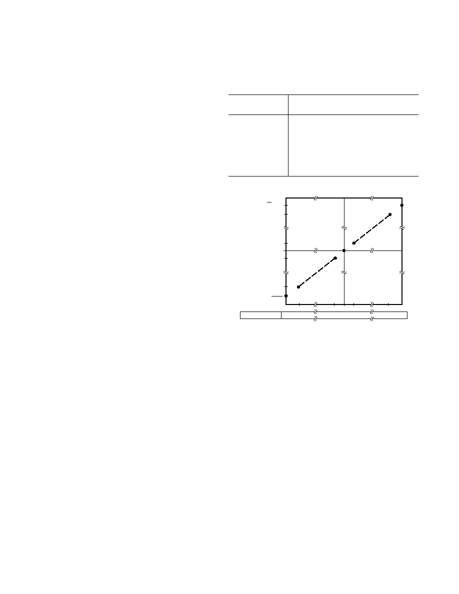
Figure 25. Main DAC Output Voltage vs. DAC Input Codes
(HEX) for Offset Binary Coding
Figure 25 shows the Main DAC transfer function when offset
binary coding is used. With offset binary coding selected the
output voltage can be calculated as follows:
VOUT' = VBIAS + 1.875
× V
BIAS
× ((NA-512)/1024)
where NA is the decimal equivalent of the offset binary input
code. NA ranges from 0 to 1023.
Table IX shows the offset binary transfer function for the Sub
DAC. Figure 26 shows the Sub DAC transfer function for
offset binary coding. Any Sub DAC output voltage can be
expressed as:
VOUT" = VBIAS/16
× [(NB-128)/256]
where NB is the decimal equivalent of the offset binary input
code. NB ranges from 0 to 255.
Table VI and Figure 22 show the analog outputs available for
the above configuration. The following is the procedure re-
quired if the complete transfer function needs to be offset
around the VBIAS point. Table VII and Figure 23 show the ana-
log output variations available from the Sub DAC.
System Control Register Write:
MODE = 0, address inputs (A2, A1, A0) are don’t cares.
Write 020 Hex
Configure part for 10-bit parallel, twos
complement coding, normal operation
Channel Control Register Write:
MODE = 0, address inputs (A2, A1, A0) select desired channel.
Write 091 Hex
Internal VDD/2 selected as VBIAS for
DAC, and any DAC data writes that
follow are to the Sub DAC.
DAC Data Register Write:
MODE = 1, address inputs (A2, A1, A0) select desired channel.
Write XX Hex
With MODE = 1 all data writes are to
the selected DACs Sub DAC. XX is the
required data. 7F Hex will give zero scale
and 80 Hex will give full scale from the
Sub DAC.
Channel Control Register Write:
MODE = 0, address inputs (A2, A1, A0) select desired channel.
Write 011 Hex
Internal VDD/2 selected as VBIAS for
DAC, and any DAC data writes that
follow are to the Main DAC.
DAC Data Register Write:
MODE = 1, address inputs (A2, A1, A0) select desired channel.
Write XXX Hex With MODE = 1 all data writes are to
the selected Main DAC. XXX is the
required data. 1FF Hex will give zero
scale and 200 Hex will give full scale
from the DAC.
相关PDF资料 |
PDF描述 |
|---|---|
| SI5367B-C-GQR | IC CLOCK MULTIPLIER PROG 100TQFP |
| SI5365-C-GQR | IC CLOCK MULTIPLIER PROG 100TQFP |
| IDT74FCT164245TPAG8 | TRANSLATOR 16BIT BIDIR 48-TSSOP |
| LTC2604CGN#PBF | IC DAC 16BIT QUAD R-R OUT 16SSOP |
| VE-20Y-MY-F2 | CONVERTER MOD DC/DC 3.3V 33W |
相关代理商/技术参数 |
参数描述 |
|---|---|
| AD7808BRZ-REEL | 功能描述:IC DAC 10BIT OCTAL SRL 24-SOIC RoHS:是 类别:集成电路 (IC) >> 数据采集 - 数模转换器 系列:- 产品培训模块:Data Converter Fundamentals DAC Architectures 标准包装:750 系列:- 设置时间:7µs 位数:16 数据接口:并联 转换器数目:1 电压电源:双 ± 功率耗散(最大):100mW 工作温度:0°C ~ 70°C 安装类型:表面贴装 封装/外壳:28-LCC(J 形引线) 供应商设备封装:28-PLCC(11.51x11.51) 包装:带卷 (TR) 输出数目和类型:1 电压,单极;1 电压,双极 采样率(每秒):143k |
| AD7808BST | 制造商:AD 制造商全称:Analog Devices 功能描述:+3.3 V to +5 V Quad/Octal 10-Bit DACs(300.12 k) |
| AD7809 | 制造商:AD 制造商全称:Analog Devices 功能描述:+3.3 V to +5 V Quad/Octal 10-Bit DACs |
| AD7809BST | 制造商:Analog Devices 功能描述:DAC 8-CH 10-bit 44-Pin TQFP 制造商:Rochester Electronics LLC 功能描述:OCTAL 10-BIT PARALLEL DAC I.C. - Bulk 制造商:Analog Devices 功能描述:IC 10-BIT DAC |
发布紧急采购,3分钟左右您将得到回复。