参数资料
| 型号: | AD7809BSTZ |
| 厂商: | Analog Devices Inc |
| 文件页数: | 13/28页 |
| 文件大小: | 0K |
| 描述: | IC DAC 10BIT OCTAL PARALL 44TQFP |
| 产品培训模块: | Data Converter Fundamentals DAC Architectures |
| 标准包装: | 1 |
| 设置时间: | 1.5µs |
| 位数: | 10 |
| 数据接口: | 并联 |
| 转换器数目: | 4 |
| 电压电源: | 模拟和数字 |
| 功率耗散(最大): | 99mW |
| 工作温度: | -40°C ~ 85°C |
| 安装类型: | 表面贴装 |
| 封装/外壳: | 44-TQFP |
| 供应商设备封装: | 44-TQFP(10x10) |
| 包装: | 托盘 |
| 输出数目和类型: | 8 电压,双极 |
| 采样率(每秒): | 667k |
| 产品目录页面: | 785 (CN2011-ZH PDF) |
第1页第2页第3页第4页第5页第6页第7页第8页第9页第10页第11页第12页当前第13页第14页第15页第16页第17页第18页第19页第20页第21页第22页第23页第24页第25页第26页第27页第28页
AD7804/AD7805/AD7808/AD7809
REV. A
–20–
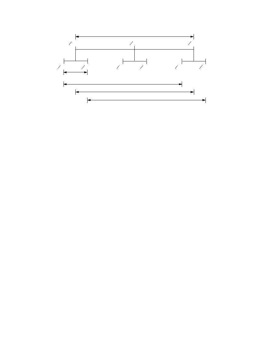
VBIAS
2
32
MAIN DAC RANGE
SUB DAC
RANGE
CHANNEL RANGE MIN CODE LOADED TO SUB DAC
CHANNEL RANGE CENTER CODE LOADED TO SUB DAC
CHANNEL RANGE MAX CODE LOADED TO SUB DAC
VBIAS
32
VBIAS
62
32
VBIAS
1
32
VBIAS
3
32
VBIAS
31
32
VBIAS
33
32
VBIAS
61
32
VBIAS
63
32
Figure 28. Pictorial View of Transfer Function for Any DAC Channel
Grounding and Layout Techniques
To obtain optimum performance from the AD7804/AD7805/
AD7808/AD7809 care should be taken with the layout. Causes
for concern would be feedthrough from the interface bus onto
the analog circuitry particularly the reference pins and ground
loops. The board should be designed such that the analog and
digital sections are separated as much as possible. Ground plan-
ing and shielding should be used as much as possible. Digital
and analog ground planes should only be joined in one place to
avoid ground loops. The ideal place to join the ground planes is
at the analog and digital ground pins of the DAC. Alternatively
a star ground should be established on the board to which all
other grounds are returned. Good decoupling is important in
achieving optimum performance. All supplies, analog or digital,
should be decoupled with 10
F tantalum and 0.1 F ceramic
capacitors to their respective grounds, and should be as close as
possible to the pins of the device. The main aim of the bypass-
ing element is to maximize the charge stored in the bypass loop
while simultaneously minimizing the inductance of this loop.
Inductance in the loop acts as an impedance to high frequency
transients and results in power supply spiking. By keeping the
decoupling as close as possible to the device, the loop area is kept
to a minimum thus reducing the possibility of power supply spikes.
On the AD7805 the REFOUT pin of the device is located next
to the DB9 of the data bus, to reduce the risk of digital feed-
through and noise being coupled from the digital section onto
the reference, the REFOUT pin and any trace connected to it
should be shielded with analog ground. To reduce the noise on
this reference it should be decoupled with a 0.01
F capacitor to
analog ground, keeping the capacitor as close as possible to the
device. The comp pin which is the output from the internal
VDD/2 reference is located next to VOUTD on the DAC and is
sensitive to noise pickup and feedthrough from the DAC output
and thus should be shielded with analog ground to keep this
reference point as quiet as possible. The comp pin should be
decoupled both to AVDD and AGND with 1–10 nF ceramic
capacitors. The external REFIN pin should also be shielded
with analog ground from the digital pins located next to it.
The same precautions should be taken with the reference pins
on the AD7804/AD7808 to reduce the risk of noise pickup and
feedthrough.
Reference Settling Time
With the REFOUT on the AD7804/AD7805/AD7808/AD7809
decoupled with a 0.01
F capacitor to AGND it takes the
REFOUT approximately 2 ms to fully settle after taking the
device out of power down. When this capacitor is reduced to
1 nF the settling time reduces to 150
s. The size of the capaci-
tor required on the REFOUT depends to a large extent on the
layout, if the REFOUT is well shielded with AGND the size of
the capacitor can be reduced thus reducing the settling time for
the reference. The internal VDD/2 reference provided at the
comp pin when decoupled with a 1 nF capacitor to both AVDD
and AGND has very fast settling time, typically less than 500 ns.
相关PDF资料 |
PDF描述 |
|---|---|
| MS3108E32-2S | CONN PLUG 5POS RT ANG W/SCKT |
| JL05-2A24-10SC-F0-R | CONN RCPT 7POS SOCKET W/OUT CONT |
| VE-24L-MY-F1 | CONVERTER MOD DC/DC 28V 50W |
| VI-J4F-MZ-F2 | CONVERTER MOD DC/DC 72V 25W |
| VI-261-MW-F2 | CONVERTER MOD DC/DC 12V 100W |
相关代理商/技术参数 |
参数描述 |
|---|---|
| AD7809BSTZ-REEL | 功能描述:IC DAC 10BIT OCTAL PARALL 44TQFP RoHS:是 类别:集成电路 (IC) >> 数据采集 - 数模转换器 系列:- 产品培训模块:Data Converter Fundamentals DAC Architectures 标准包装:750 系列:- 设置时间:7µs 位数:16 数据接口:并联 转换器数目:1 电压电源:双 ± 功率耗散(最大):100mW 工作温度:0°C ~ 70°C 安装类型:表面贴装 封装/外壳:28-LCC(J 形引线) 供应商设备封装:28-PLCC(11.51x11.51) 包装:带卷 (TR) 输出数目和类型:1 电压,单极;1 电压,双极 采样率(每秒):143k |
| AD780AN | 功能描述:IC VREF SERIES SHUNT PREC 8-PDIP RoHS:否 类别:集成电路 (IC) >> PMIC - 电压基准 系列:- 标准包装:3,000 系列:- 基准类型:旁路,精度 输出电压:5V 容差:±0.5% 温度系数:100ppm/°C 输入电压:- 通道数:1 电流 - 阴极:80µA 电流 - 静态:- 电流 - 输出:15mA 工作温度:-40°C ~ 85°C 安装类型:表面贴装 封装/外壳:TO-236-3,SC-59,SOT-23-3 供应商设备封装:SOT-23-3 包装:带卷 (TR) 其它名称:LM4040CIM3-5.0MLTRLM4040CIM3-5.0MLTR-ND |
| AD780ANZ | 功能描述:IC VREF SERIES SHUNT PREC 8-PDIP RoHS:是 类别:集成电路 (IC) >> PMIC - 电压基准 系列:- 标准包装:3,000 系列:- 基准类型:旁路,精度 输出电压:3V 容差:±0.5% 温度系数:100ppm/°C 输入电压:- 通道数:1 电流 - 阴极:82µA 电流 - 静态:- 电流 - 输出:15mA 工作温度:-40°C ~ 85°C 安装类型:表面贴装 封装/外壳:6-TSSOP(5 引线),SC-88A,SOT-353 供应商设备封装:SC-70-5 包装:带卷 (TR) 其它名称:296-20888-2 |
| AD780AR | 功能描述:IC VREF SERIES SHUNT PREC 8-SOIC RoHS:否 类别:集成电路 (IC) >> PMIC - 电压基准 系列:- 标准包装:2,000 系列:- 基准类型:旁路,可调节,精度 输出电压:1.24 V ~ 16 V 容差:±0.5% 温度系数:- 输入电压:1.24 V ~ 16 V 通道数:1 电流 - 阴极:100µA 电流 - 静态:- 电流 - 输出:20mA 工作温度:-40°C ~ 85°C 安装类型:通孔 封装/外壳:TO-226-3、TO-92-3(TO-226AA)成形引线 供应商设备封装:TO-92-3 包装:带卷 (TR) |
| AD780AR-REEL7 | 功能描述:IC VREF SERIES SHUNT PREC 8-SOIC RoHS:否 类别:集成电路 (IC) >> PMIC - 电压基准 系列:- 标准包装:2,000 系列:- 基准类型:旁路,可调节,精度 输出电压:1.24 V ~ 16 V 容差:±0.5% 温度系数:- 输入电压:1.24 V ~ 16 V 通道数:1 电流 - 阴极:100µA 电流 - 静态:- 电流 - 输出:20mA 工作温度:-40°C ~ 85°C 安装类型:通孔 封装/外壳:TO-226-3、TO-92-3(TO-226AA)成形引线 供应商设备封装:TO-92-3 包装:带卷 (TR) |
发布紧急采购,3分钟左右您将得到回复。