- 您现在的位置:买卖IC网 > PDF目录10296 > AD7813YNZ (Analog Devices Inc)IC ADC 10BIT PARALLEL 16-DIP PDF资料下载
参数资料
| 型号: | AD7813YNZ |
| 厂商: | Analog Devices Inc |
| 文件页数: | 8/11页 |
| 文件大小: | 0K |
| 描述: | IC ADC 10BIT PARALLEL 16-DIP |
| 标准包装: | 25 |
| 位数: | 10 |
| 采样率(每秒): | 400k |
| 数据接口: | 并联 |
| 转换器数目: | 1 |
| 功率耗散(最大): | 17.5mW |
| 电压电源: | 单电源 |
| 工作温度: | -40°C ~ 105°C |
| 安装类型: | 通孔 |
| 封装/外壳: | 16-DIP(0.300",7.62mm) |
| 供应商设备封装: | 16-PDIP |
| 包装: | 管件 |
| 输入数目和类型: | 1 个单端,单极 |
AD7813
–6–
REV. C
CIRCUIT DESCRIPTION
Converter Operation
The AD7813 is a successive approximation analog-to-digital
converter based around a charge redistribution DAC. The ADC
can convert analog input signals in the range 0 V to VDD. Fig-
ures 2 and 3 below show simplified schematics of the ADC.
Figure 2 shows the ADC during its acquisition phase. SW2 is
closed and SW1 is in Position A, the comparator is held in a
balanced condition and the sampling capacitor acquires the
signal on VIN+.
CHARGE
REDISTRIBUTION
DAC
CONTROL
LOGIC
CLOCK
OSC
COMPARATOR
SW2
VDD/3
ACQUISITION
PHASE
SAMPLING
CAPACITOR
SW1
A
B
AGND
VIN+
Figure 2. ADC Track Phase
When the ADC starts a conversion (see Figure 3), SW2 will
open and SW1 will move to Position B, causing the comparator
to become unbalanced. The Control Logic and the Charge
Redistribution DAC are used to add and subtract fixed amounts
of charge from the sampling capacitor so as to bring the compara-
tor back into a balanced condition. When the comparator is
rebalanced the conversion is complete. The Control Logic gen-
erates the ADC output code. Figure 7 shows the ADC transfer
function.
CHARGE
REDISTRIBUTION
DAC
CONTROL
LOGIC
CLOCK
OSC
COMPARATOR
SW2
VDD/3
CONVERSION
PHASE
SAMPLING
CAPACITOR
SW1
A
B
AGND
VIN+
Figure 3. ADC Conversion Phase
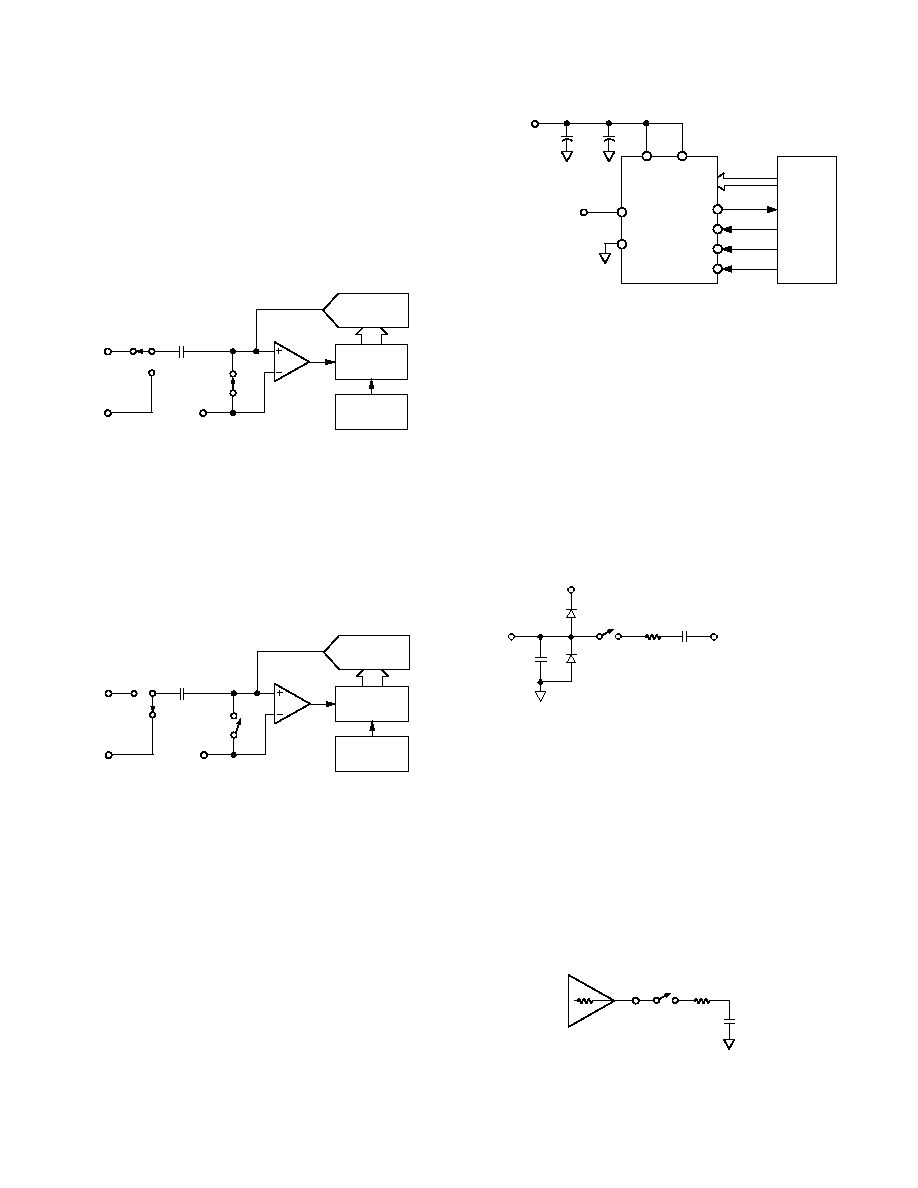
TYPICAL CONNECTION DIAGRAM
Figure 4 shows a typical connection diagram for the AD7813. The
parallel interface is implemented using an 8-bit data bus, the
falling edge of CONVST brings the BUSY signal high, and at
the end of conversion the falling edge of BUSY is used to ini-
tiate an Interrupt Service Routine (ISR) on a microprocessor—
see Parallel Interface section for more details. VREF is connected
to a well decoupled VDD pin to provide an analog input range of
0 V to VDD. When VDD is first connected the AD7813 powers
up in a low current mode, i.e., power-down. A rising edge on an
internal CONVST input will cause the part to power up—see
Power-Up Times. If power consumption is of concern, the
automatic power-down at the end of a conversion should be
used to improve power performance. See Power vs. Throughput
Rate section of the data sheet.
BUSY
RD
CS
CONVST
DB0-DB7
VDD
VREF
VIN
GND
AD7813
C/ P
PARALLEL
INTERFACE
0V TO VREF
INPUT
0.1 F
10 F
SUPPLY
2.7V TO 5.5V
Figure 4. Typical Connection Diagram
Analog Input
Figure 5 shows an equivalent circuit of the analog input struc-
ture of the AD7813. The two diodes, D1 and D2, provide ESD
protection for the analog inputs. Care must be taken to ensure
that the analog input signal never exceeds the supply rails by
more than 200 mV. This will cause these diodes to become
forward biased and start conducting current into the substrate.
The maximum current these diodes can conduct without caus-
ing irreversible damage to the part is 20 mA. The capacitor C2,
in Figure 5, is typically about 4 pF and can be primarily attrib-
uted to pin capacitance. The resistor R1 is a lumped component
made up of the on resistance of a multiplexer and a switch. This
resistor is typically about 125
. The capacitor C1 is the ADC
sampling capacitor and has a capacitance of 3.5 pF.
VDD
VIN
C2
4pF
D1
D2
R1
125
C1
3.5pF
VDD/3
CONVERT PHASE – SWITCH OPEN
TRACK PHASE – SWITCH CLOSED
Figure 5. Equivalent Analog Input Circuit
DC Acquisition Time
The ADC starts a new acquisition phase at the end of a conver-
sion and ends on the falling edge of the CONVST signal. At the
end of a conversion there is a settling time associated with the
sampling circuit. This settling time lasts approximately 100 ns.
The analog signal on VIN is also being acquired during this settling
time; therefore, the minimum acquisition time needed is
approximately 100 ns.
Figure 6 shows the equivalent charging circuit for the sampling
capacitor when the ADC is in its acquisition phase. R2 repre-
sents the source impedance of a buffer amplifier or resistive
network, R1 is an internal multiplexer resistance and C1 is the
sampling capacitor.
VIN
R1
125
R2
C1
3.5pF
Figure 6. Equivalent Sampling Circuit
相关PDF资料 |
PDF描述 |
|---|---|
| AD7708BRZ-REEL7 | IC ADC 16BIT R-R 8/10CH 28SOIC |
| CS3100A-14S-78P | CONN RCPT 2POS WALL MNT W/PINS |
| AD7366BRUZ-5-RL7 | IC ADC 12BIT DUAL BIPO 24-TSSOP |
| MS27467E21B11BA | CONN HSG PLUG 11POS STRGHT SCKT |
| D38999/26MD19SNLC | CONN HSG PLUG 19POS STRGHT SCKT |
相关代理商/技术参数 |
参数描述 |
|---|---|
| AD7813YR | 制造商:Analog Devices 功能描述:ADC Single SAR 400ksps 10-bit Parallel 16-Pin SOIC N 制造商:Analog Devices 功能描述:IC 10-BIT ADC |
| AD7813YR-REEL | 制造商:Analog Devices 功能描述:ADC Single SAR 400ksps 10-bit Parallel 16-Pin SOIC N T/R |
| AD7813YR-REEL7 | 制造商:Analog Devices 功能描述:ADC Single SAR 400ksps 10-bit Parallel 16-Pin SOIC N T/R |
| AD7813YRU | 功能描述:IC ADC 10BIT PARALLEL 16-TSSOP RoHS:否 类别:集成电路 (IC) >> 数据采集 - 模数转换器 系列:- 产品培训模块:Lead (SnPb) Finish for COTS Obsolescence Mitigation Program 标准包装:2,500 系列:- 位数:12 采样率(每秒):3M 数据接口:- 转换器数目:- 功率耗散(最大):- 电压电源:- 工作温度:- 安装类型:表面贴装 封装/外壳:SOT-23-6 供应商设备封装:SOT-23-6 包装:带卷 (TR) 输入数目和类型:- |
| AD7813YRU-REEL | 制造商:Analog Devices 功能描述:ADC Single SAR 400ksps 10-bit Parallel 16-Pin TSSOP T/R 制造商:Analog Devices 功能描述:ADC SGL SAR 400KSPS 10-BIT PARALLEL 16TSSOP - Tape and Reel |
发布紧急采购,3分钟左右您将得到回复。