- 您现在的位置:买卖IC网 > PDF目录10298 > AD7813YRUZ (Analog Devices Inc)IC ADC 10BIT PARALLEL 16TSSOP PDF资料下载
参数资料
| 型号: | AD7813YRUZ |
| 厂商: | Analog Devices Inc |
| 文件页数: | 10/11页 |
| 文件大小: | 0K |
| 描述: | IC ADC 10BIT PARALLEL 16TSSOP |
| 标准包装: | 96 |
| 位数: | 10 |
| 采样率(每秒): | 400k |
| 数据接口: | 并联 |
| 转换器数目: | 1 |
| 功率耗散(最大): | 17.5mW |
| 电压电源: | 单电源 |
| 工作温度: | -40°C ~ 105°C |
| 安装类型: | 表面贴装 |
| 封装/外壳: | 16-TSSOP(0.173",4.40mm 宽) |
| 供应商设备封装: | 16-TSSOP |
| 包装: | 管件 |
| 输入数目和类型: | 1 个单端,单极 |
AD7813
–8–
REV. C
Typical Performance Characteristics
THROUGHPUT – kSPS
POWER
–
mW
10
1
0.01
050
5
10152025
30
3540
45
0.1
Figure 10. Power vs. Throughput
0
–60
–100
dBs
–10
–50
–70
–90
–30
–40
–80
–20
FREQUENCY – kHz
0
174
17
35
52
70
87
105
122
140
157
AD7813
2048 POINT FFT
SAMPLING 357.142kHz
fIN 30.168kHz
Figure 11. SNR
TIMING AND CONTROL
The AD7813 has only one input for timing and control, i.e.,
the CONVST (convert start signal). The rising edge of this
CONVST signal initiates a 1.5
s pulse on an internally gener-
ated CONVST signal. This pulse is present to ensure the part
has enough time to power up before a conversion is initiated. If
the external CONVST signal is low, the falling edge of the
internal CONVST signal will cause the sampling circuit to go
into hold mode and initiate a conversion. If, however, the exter-
nal CONVST signal is high when the internal CONVST goes
low, it is upon the falling edge of the external CONVST signal
that the sampling circuitry will go into hold mode and initiate a
conversion. The use of the internally generated 1.5
s pulse,
as previously described, can be likened to the configuration
shown in Figure 12. The application of a CONVST signal at
the CONVST pin triggers the generation of a 1.5
s pulse. Both
the external CONVST and this internal CONVST are input to
an OR gate. The resulting signal has the duration of the longer
of the two input signals. Once a conversion has been initiated
the BUSY signal goes high to indicate a conversion is in progress.
At the end of conversion the sampling circuit goes back into its
tracking mode again. The end of conversion is indicated by the
BUSY signal going low. This signal may be used to initiate an
ISR on a microprocessor. At this point the conversion result is
latched into the output register where it may be read. The AD7813
has an 8-bit wide parallel interface. The 10-bit conversion result
is accessed by performing two successive read operations. The
first 8-bit read accesses the 8 MSBs of the conversion result and
the second read accesses the 2 LSBs, as illustrated in Figure 13,
where one performance of the two successive reads is highlighted
after the falling edge of BUSY. The state of the external CONVST
signal at the end of conversion also establishes the mode of opera-
tion of the AD7813.
Mode 1 Operation (High Speed Sampling)
If the external CONVST is logic high when BUSY goes low, the
part is said to be in Mode 1 operation. While operating in Mode
1, the AD7813 will not power down between conversions. The
AD7813 should be operated in Mode 1 for high speed sampling
applications, i.e., throughputs greater than 100 kSPS. Figure 13
shows the timing for Mode 1 operation. From this diagram one
can see that a minimum delay of the sum of the conversion time
and read time must be left between two successive falling edges
of the external CONVST. This is to ensure that a conversion is
not initiated during a read.
Mode 2 Operation (Automatic Power-Down)
At slower throughput rates the AD7813 may be powered down
between conversions to give a superior power performance.
This is Mode 2 Operation and it is achieved by bringing the
CONVST signal logic low before the falling edge of BUSY.
Figure 14, overleaf, shows the timing for Mode 2 Operation.
The falling edge of the external CONVST signal may occur
before or after the falling edge of the internal CONVST signal,
but it is the later occurring falling edge of both that controls
when the first conversion will take place. If the falling edge
of the external CONVST occurs after that of the internal
CONVST, it means that the moment of the first conversion is
controlled exactly, regardless of any jitter associated with the
internal CONVST signal. The parallel interface is still fully
operational while the AD7813 is powered down. The AD7813
is powered up again on the rising edge of the CONVST signal.
The gated CONVST pulse will now remain high long enough
for the AD7813 to fully power up, which takes about 1.5
s. This
is ensured by the internal CONVST signal, which will remain high
for 1.5
s.
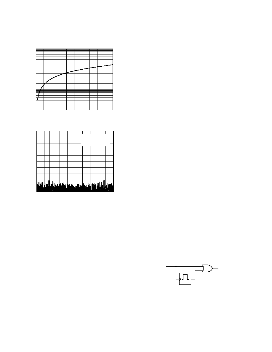
1.5 s
EXT
INT
CONVST
(PIN 4)
GATED
Figure 12.
相关PDF资料 |
PDF描述 |
|---|---|
| MS27656T25B24B | CONN HSG RCPT 24POS WALL MT SCKT |
| D38999/26JF32PNLC | CONN HSG PLUG 32POS STRGHT PINS |
| VE-B3N-MY | CONVERTER MOD DC/DC 18.5V 50W |
| D38999/20WJ4AA | CONN HSG RCPT 56POS WALL MT PINS |
| VE-B3M-MY | CONVERTER MOD DC/DC 10V 50W |
相关代理商/技术参数 |
参数描述 |
|---|---|
| AD7813YRUZ-REEL | 制造商:Analog Devices 功能描述:ADC Single SAR 400ksps 10-bit Parallel 16-Pin TSSOP T/R 制造商:Analog Devices 功能描述:ADC SGL SAR 400KSPS 10-BIT PARALLEL 16TSSOP - Tape and Reel |
| AD7813YRUZ-REEL7 | 功能描述:IC ADC 10BIT PARALLEL 16TSSOP RoHS:是 类别:集成电路 (IC) >> 数据采集 - 模数转换器 系列:- 标准包装:2,500 系列:- 位数:16 采样率(每秒):15 数据接口:MICROWIRE?,串行,SPI? 转换器数目:1 功率耗散(最大):480µW 电压电源:单电源 工作温度:-40°C ~ 85°C 安装类型:表面贴装 封装/外壳:38-WFQFN 裸露焊盘 供应商设备封装:38-QFN(5x7) 包装:带卷 (TR) 输入数目和类型:16 个单端,双极;8 个差分,双极 配用:DC1011A-C-ND - BOARD DELTA SIGMA ADC LTC2494 |
| AD7813YRZ | 功能描述:IC ADC 10BIT PARALLEL 16-SOIC RoHS:是 类别:集成电路 (IC) >> 数据采集 - 模数转换器 系列:- 标准包装:1,000 系列:- 位数:16 采样率(每秒):45k 数据接口:串行 转换器数目:2 功率耗散(最大):315mW 电压电源:模拟和数字 工作温度:0°C ~ 70°C 安装类型:表面贴装 封装/外壳:28-SOIC(0.295",7.50mm 宽) 供应商设备封装:28-SOIC W 包装:带卷 (TR) 输入数目和类型:2 个单端,单极 |
| AD7813YRZ-REEL | 功能描述:IC ADC 10BIT PARALLEL 16SOIC RoHS:是 类别:集成电路 (IC) >> 数据采集 - 模数转换器 系列:- 标准包装:2,500 系列:- 位数:16 采样率(每秒):15 数据接口:MICROWIRE?,串行,SPI? 转换器数目:1 功率耗散(最大):480µW 电压电源:单电源 工作温度:-40°C ~ 85°C 安装类型:表面贴装 封装/外壳:38-WFQFN 裸露焊盘 供应商设备封装:38-QFN(5x7) 包装:带卷 (TR) 输入数目和类型:16 个单端,双极;8 个差分,双极 配用:DC1011A-C-ND - BOARD DELTA SIGMA ADC LTC2494 |
| AD7813YRZ-REEL7 | 功能描述:IC ADC 10BIT PARALLEL 16SOIC RoHS:是 类别:集成电路 (IC) >> 数据采集 - 模数转换器 系列:- 标准包装:2,500 系列:- 位数:16 采样率(每秒):15 数据接口:MICROWIRE?,串行,SPI? 转换器数目:1 功率耗散(最大):480µW 电压电源:单电源 工作温度:-40°C ~ 85°C 安装类型:表面贴装 封装/外壳:38-WFQFN 裸露焊盘 供应商设备封装:38-QFN(5x7) 包装:带卷 (TR) 输入数目和类型:16 个单端,双极;8 个差分,双极 配用:DC1011A-C-ND - BOARD DELTA SIGMA ADC LTC2494 |
发布紧急采购,3分钟左右您将得到回复。