- 您现在的位置:买卖IC网 > PDF目录10298 > AD7813YRUZ (Analog Devices Inc)IC ADC 10BIT PARALLEL 16TSSOP PDF资料下载
参数资料
| 型号: | AD7813YRUZ |
| 厂商: | Analog Devices Inc |
| 文件页数: | 5/11页 |
| 文件大小: | 0K |
| 描述: | IC ADC 10BIT PARALLEL 16TSSOP |
| 标准包装: | 96 |
| 位数: | 10 |
| 采样率(每秒): | 400k |
| 数据接口: | 并联 |
| 转换器数目: | 1 |
| 功率耗散(最大): | 17.5mW |
| 电压电源: | 单电源 |
| 工作温度: | -40°C ~ 105°C |
| 安装类型: | 表面贴装 |
| 封装/外壳: | 16-TSSOP(0.173",4.40mm 宽) |
| 供应商设备封装: | 16-TSSOP |
| 包装: | 管件 |
| 输入数目和类型: | 1 个单端,单极 |
AD7813
–3–
REV. C
ORDERING GUIDE
Linearity Package
Package
Model
Error
Description
Option
AD7813YN
±1 LSB
Plastic DIP
N-16
AD7813YR
±1 LSB
Small Outline IC
R-16A
AD7813YRU
±1 LSB
Thin Shrink Small Outline RU-16
(TSSOP)
TIMING CHARACTERISTICS
1, 2
Parameter
V
DD = 3 V
10%
V
DD = 5 V
10%
Unit
Conditions/Comments
tPOWER-UP
1.5
s (max)
Power-Up Time of AD7813 after Rising Edge of CONVST.
t1
2.3
s (max)
Conversion Time.
t2
20
ns (min)
CONVST Pulsewidth.
t3
30
ns (max)
CONVST Falling Edge to BUSY Rising Edge Delay.
t4
0
ns (min)
CS to RD Setup Time.
t5
0
ns (min)
CS Hold Time after RD High.
t6
3
10
ns (max)
Data Access Time after RD Low.
t7
3, 4
10
ns (max)
Bus Relinquish Time after RD High.
5
ns (min)
t8
10
ns (min)
Minimum Time Between MSB and LSB Reads.
t9
3
50
ns (min)
Rising Edge of CS or RD to Falling Edge of CONVST Delay.
NOTES
1Sample tested to ensure compliance.
2See Figures 12, 13 and 14.
3These numbers are measured with the load circuit of Figure 1. They are defined as the time required for the o/p to cross 0.8 V or 2.4 V for V
DD = 5 V
± 10% and
0.4 V or 2 V for VDD = 3 V
± 10%.
4Derived from the measured time taken by the data outputs to change 0.5 V when loaded with the circuit of Figure 1. The measured number is then extrapolated back
to remove the effects of charging or discharging the 50 pF capacitor. This means that the time, t 7, quoted in the Timing Characteristics is the true bus relinquish time
of the part and as such is independent of external bus loading capacitances.
(–40 C to +105 C, unless otherwise noted)
ABSOLUTE MAXIMUM RATINGS
*
VDD to DGND . . . . . . . . . . . . . . . . . . . . . . . . . –0.3 V to +7 V
Digital Input Voltage to DGND
(CONVST, RD, CS) . . . . . . . . . . . . . . –0.3 V, VDD + 0.3 V
Digital Output Voltage to DGND
(BUSY, DB0–DB7) . . . . . . . . . . . . . . . –0.3 V, VDD + 0.3 V
REFIN to AGND . . . . . . . . . . . . . . . . . . . –0.3 V, VDD + 0.3 V
Analog Input . . . . . . . . . . . . . . . . . . . . . . –0.3 V, VDD + 0.3 V
Storage Temperature Range . . . . . . . . . . . . –65
°C to +150°C
Junction Temperature . . . . . . . . . . . . . . . . . . . . . . . . . . 150
°C
Plastic DIP Package, Power Dissipation . . . . . . . . . . 450 mW
θJA Thermal Impedance . . . . . . . . . . . . . . . . . . . . 105°C/W
Lead Temperature, (Soldering 10 sec) . . . . . . . . . . . . 260
°C
SOIC Package, Power Dissipation . . . . . . . . . . . . . . . 450 mW
θJA Thermal Impedance . . . . . . . . . . . . . . . . . . . . . 75°C/W
Lead Temperature, Soldering
Vapor Phase (60 sec) . . . . . . . . . . . . . . . . . . . . . . . 215
°C
Infrared (15 sec) . . . . . . . . . . . . . . . . . . . . . . . . . . 220
°C
SSOP Package, Power Dissipation . . . . . . . . . . . . . . . 450 mW
θJA Thermal Impedance . . . . . . . . . . . . . . . . . . . . 115°C/W
Lead Temperature, Soldering
Vapor Phase (60 sec) . . . . . . . . . . . . . . . . . . . . . . . 215
°C
Infrared (15 sec) . . . . . . . . . . . . . . . . . . . . . . . . . . 220
°C
*Stresses above those listed under Absolute Maximum Ratings may cause perma-
nent damage to the device. This is a stress rating only; functional operation of the
device at these or any other conditions above those listed in the operational sections
of this specification is not implied. Exposure to absolute maximum rating condi-
tions for extended periods may affect device reliability.
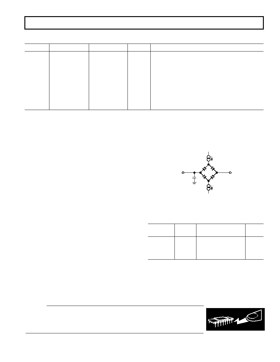
1.6V
200 AIOL
200 A
IOH
CL
50pF
TO
OUTPUT
PIN
Figure 1. Load Circuit for Digital Output Timing
Specifications
CAUTION
ESD (electrostatic discharge) sensitive device. Electrostatic charges as high as 4000 V readily
accumulate on the human body and test equipment and can discharge without detection. Although
the AD7813 features proprietary ESD protection circuitry, permanent damage may occur on
devices subjected to high-energy electrostatic discharges. Therefore, proper ESD precautions are
recommended to avoid performance degradation or loss of functionality.
WARNING!
ESD SENSITIVE DEVICE
相关PDF资料 |
PDF描述 |
|---|---|
| MS27656T25B24B | CONN HSG RCPT 24POS WALL MT SCKT |
| D38999/26JF32PNLC | CONN HSG PLUG 32POS STRGHT PINS |
| VE-B3N-MY | CONVERTER MOD DC/DC 18.5V 50W |
| D38999/20WJ4AA | CONN HSG RCPT 56POS WALL MT PINS |
| VE-B3M-MY | CONVERTER MOD DC/DC 10V 50W |
相关代理商/技术参数 |
参数描述 |
|---|---|
| AD7813YRUZ-REEL | 制造商:Analog Devices 功能描述:ADC Single SAR 400ksps 10-bit Parallel 16-Pin TSSOP T/R 制造商:Analog Devices 功能描述:ADC SGL SAR 400KSPS 10-BIT PARALLEL 16TSSOP - Tape and Reel |
| AD7813YRUZ-REEL7 | 功能描述:IC ADC 10BIT PARALLEL 16TSSOP RoHS:是 类别:集成电路 (IC) >> 数据采集 - 模数转换器 系列:- 标准包装:2,500 系列:- 位数:16 采样率(每秒):15 数据接口:MICROWIRE?,串行,SPI? 转换器数目:1 功率耗散(最大):480µW 电压电源:单电源 工作温度:-40°C ~ 85°C 安装类型:表面贴装 封装/外壳:38-WFQFN 裸露焊盘 供应商设备封装:38-QFN(5x7) 包装:带卷 (TR) 输入数目和类型:16 个单端,双极;8 个差分,双极 配用:DC1011A-C-ND - BOARD DELTA SIGMA ADC LTC2494 |
| AD7813YRZ | 功能描述:IC ADC 10BIT PARALLEL 16-SOIC RoHS:是 类别:集成电路 (IC) >> 数据采集 - 模数转换器 系列:- 标准包装:1,000 系列:- 位数:16 采样率(每秒):45k 数据接口:串行 转换器数目:2 功率耗散(最大):315mW 电压电源:模拟和数字 工作温度:0°C ~ 70°C 安装类型:表面贴装 封装/外壳:28-SOIC(0.295",7.50mm 宽) 供应商设备封装:28-SOIC W 包装:带卷 (TR) 输入数目和类型:2 个单端,单极 |
| AD7813YRZ-REEL | 功能描述:IC ADC 10BIT PARALLEL 16SOIC RoHS:是 类别:集成电路 (IC) >> 数据采集 - 模数转换器 系列:- 标准包装:2,500 系列:- 位数:16 采样率(每秒):15 数据接口:MICROWIRE?,串行,SPI? 转换器数目:1 功率耗散(最大):480µW 电压电源:单电源 工作温度:-40°C ~ 85°C 安装类型:表面贴装 封装/外壳:38-WFQFN 裸露焊盘 供应商设备封装:38-QFN(5x7) 包装:带卷 (TR) 输入数目和类型:16 个单端,双极;8 个差分,双极 配用:DC1011A-C-ND - BOARD DELTA SIGMA ADC LTC2494 |
| AD7813YRZ-REEL7 | 功能描述:IC ADC 10BIT PARALLEL 16SOIC RoHS:是 类别:集成电路 (IC) >> 数据采集 - 模数转换器 系列:- 标准包装:2,500 系列:- 位数:16 采样率(每秒):15 数据接口:MICROWIRE?,串行,SPI? 转换器数目:1 功率耗散(最大):480µW 电压电源:单电源 工作温度:-40°C ~ 85°C 安装类型:表面贴装 封装/外壳:38-WFQFN 裸露焊盘 供应商设备封装:38-QFN(5x7) 包装:带卷 (TR) 输入数目和类型:16 个单端,双极;8 个差分,双极 配用:DC1011A-C-ND - BOARD DELTA SIGMA ADC LTC2494 |
发布紧急采购,3分钟左右您将得到回复。