- 您现在的位置:买卖IC网 > PDF目录9778 > AD7827BRZ-REEL7 (Analog Devices Inc)IC ADC 8BIT SAMPLING SRL 8SOIC PDF资料下载
参数资料
| 型号: | AD7827BRZ-REEL7 |
| 厂商: | Analog Devices Inc |
| 文件页数: | 6/12页 |
| 文件大小: | 0K |
| 描述: | IC ADC 8BIT SAMPLING SRL 8SOIC |
| 产品变化通告: | AD7827 Series Discontinuation 18/Jul/2012 |
| 标准包装: | 1,000 |
| 位数: | 8 |
| 采样率(每秒): | 1M |
| 数据接口: | DSP,串行 |
| 转换器数目: | 1 |
| 功率耗散(最大): | 30mW |
| 电压电源: | 单电源 |
| 工作温度: | -40°C ~ 105°C |
| 安装类型: | 表面贴装 |
| 封装/外壳: | 8-SOIC(0.154",3.90mm 宽) |
| 供应商设备封装: | 8-SOIC |
| 包装: | 带卷 (TR) |
| 输入数目和类型: | 1 个单端,单极 |
–3–
REV. 0
AD7827
TIMING CHARACTERISTICS1, 2 (V
REFIN/REFOUT = 2.5 V, all specifications –40 C to +105 C, unless otherwise noted)
Parameter
5 V
10%
3 V
10%
Units
Conditions/Comments
tCONVERT
420
ns max
Conversion Time.
t1
20
ns min
Minimum
CONVST Pulsewidth.
t2
tCONVERT+t3
ns min
Falling edge of
CONVST to falling edge of RFS.
tCONVERT+t3+t7+t8
ns max
t3
3
14
18
ns max
Rising edge of SCLK to falling edge of RFS.
t4
14
18
ns max
Rising edge of SCLK to rising edge of RFS.
t5
3
20
ns max
Rising edge of SCLK to high impedance disabled.
t6
3
14
18
ns max
Rising edge of SCLK to DOUT valid delay.
t7
25
ns min
Minimum high SCLK pulse duration.
t8
25
ns min
Minimum low SCLK pulse duration.
t9
4
20
ns min
Bus relinquish time after SCLK falling edge.
35
ns max
t10
20
ns max
Maximum delay from falling edge
CONVST to rising edge RFS if
RFS reset by
CONVST.
t11
30
ns min
Minimum time between end of serial read and next falling edge of
CONVST.
tPOWER-UP
11
s max
Power-up time from rising edge of
CONVST using external 2.5 V
reference.
tPOWER-UP
25
s max
Power-up time from rising edge of
CONVST using on-chip reference.
NOTES
1Sample tested to ensure compliance.
2See Figures 13, 14 and 15.
3Measured with the load circuit of Figure 1 and defined as the time required for an output to cross 0.8 V or 2.4 V with V
DD = 5 V ± 10% and time required for an
output to cross 0.4 V or 2.0 V with VDD = 3 V ± 10%.
4Derived from the measured time taken by the data outputs to change 0.5 V when loaded with the circuit of Figure 1. The measured number is then extrapolated back
to remove the effects of charging or discharging the 50 pF capacitor. This means that the time, t 9, quoted in the timing characteristics is the true bus relinquish time of
the part and as such is independent of external bus loading capacitances.
Specifications subject to change without notice.
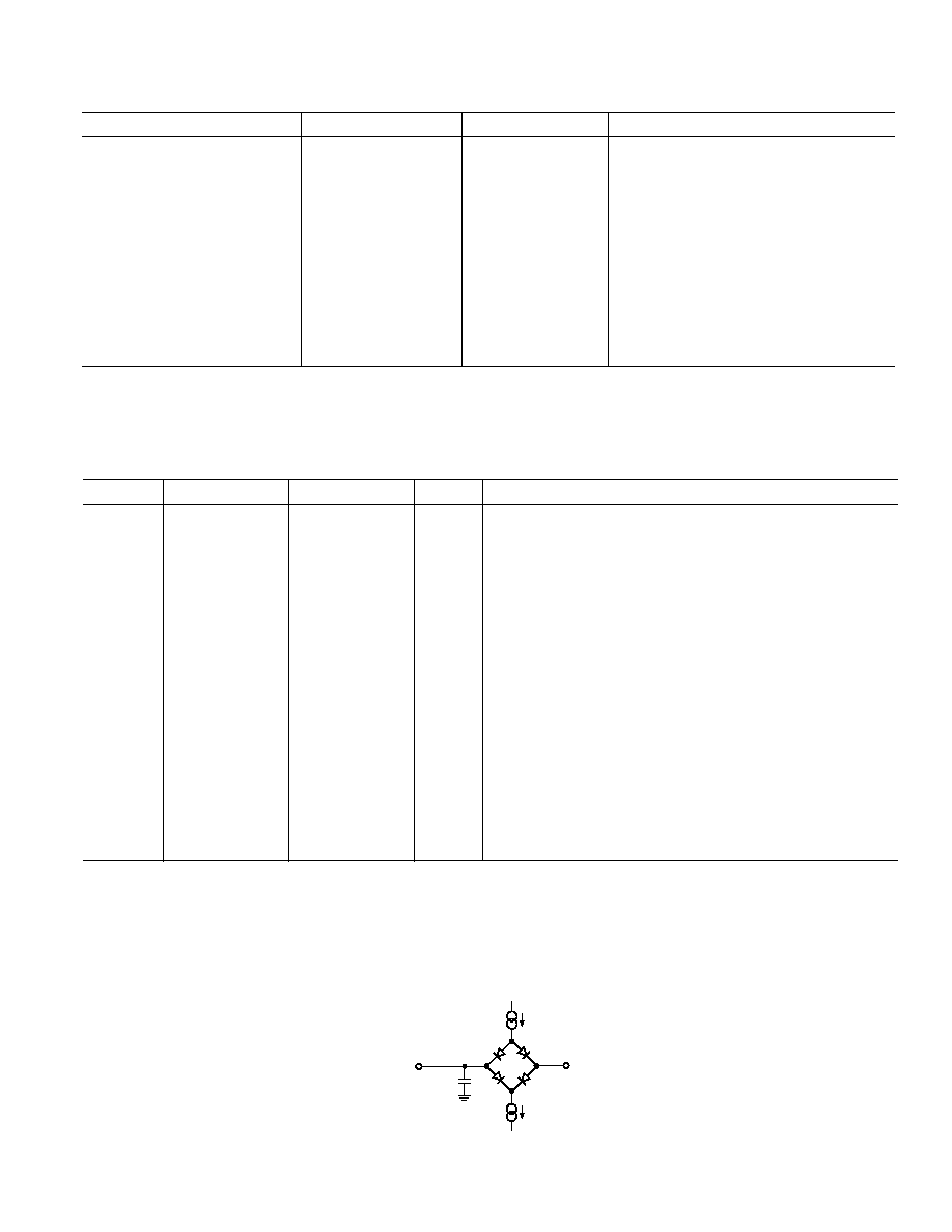
CL
50pF
TO
OUTPUT
PIN
IOL
IOH
200 A
+2.1V
Figure 1. Load Circuit for Digital Output Timing Specifications
Parameter
Version B
Units
Test Conditions/Comments
POWER SUPPLY
VDD
4.5
V min
5 V
± 10% For Specified Performance
5.5
V max
2.7
V min
3 V
± 10% For Specified Performance
3.3
V max
IDD
Normal Operation
10
mA max
8 mA Typically
Power-Down
1
A max
Logic Inputs = 0 V or VDD
Power Dissipation
VDD = 3 V
Normal Operation
30
mW max
Typically 24 mW
Power-Down
200 kSPS
9.58
mW max
1 MSPS
47.88
mW max
NOTES
1See Terminology section of this data sheet.
2Refer to the Analog Input section for an explanation of the Analog Input(s).
Specifications subject to change without notice.
相关PDF资料 |
PDF描述 |
|---|---|
| V300C15M150BG3 | CONVERTER MOD DC/DC 15V 150W |
| AD7572AJRZ10-REEL | IC ADC 12BIT HS LC2MOS 24SOIC |
| V300C15M150BG2 | CONVERTER MOD DC/DC 15V 150W |
| VE-244-MX-F3 | CONVERTER MOD DC/DC 48V 75W |
| SY10EP16VZG TR | IC RCVR HS DIFF 3.3/5V 8SOIC |
相关代理商/技术参数 |
参数描述 |
|---|---|
| AD7828 | 制造商:AD 制造商全称:Analog Devices 功能描述:LC2MOS High Speed 4- & 8-Channel 8-Bit ADCs |
| AD7828BCHIPS | 制造商:未知厂家 制造商全称:未知厂家 功能描述:Single-Ended Data Acquisition System |
| AD7828BQ | 功能描述:IC ADC 8BIT 8CH HS 28-CDIP RoHS:否 类别:集成电路 (IC) >> 数据采集 - 模数转换器 系列:- 标准包装:1 系列:- 位数:14 采样率(每秒):83k 数据接口:串行,并联 转换器数目:1 功率耗散(最大):95mW 电压电源:双 ± 工作温度:0°C ~ 70°C 安装类型:通孔 封装/外壳:28-DIP(0.600",15.24mm) 供应商设备封装:28-PDIP 包装:管件 输入数目和类型:1 个单端,双极 |
| AD7828BR | 功能描述:IC ADC 8BIT 8CH HS 28-SOIC RoHS:否 类别:集成电路 (IC) >> 数据采集 - 模数转换器 系列:- 标准包装:1,000 系列:- 位数:12 采样率(每秒):300k 数据接口:并联 转换器数目:1 功率耗散(最大):75mW 电压电源:单电源 工作温度:0°C ~ 70°C 安装类型:表面贴装 封装/外壳:24-SOIC(0.295",7.50mm 宽) 供应商设备封装:24-SOIC 包装:带卷 (TR) 输入数目和类型:1 个单端,单极;1 个单端,双极 |
| AD7828BR-REEL | 制造商:Analog Devices 功能描述:ADC Single Semiflash 50ksps 8-bit Parallel 28-Pin SOIC W T/R 制造商:Analog Devices 功能描述:CONVERTER I.C. - Tape and Reel |
发布紧急采购,3分钟左右您将得到回复。