- 您现在的位置:买卖IC网 > PDF目录10178 > AD7828BR (Analog Devices Inc)IC ADC 8BIT 8CH HS 28-SOIC PDF资料下载
参数资料
| 型号: | AD7828BR |
| 厂商: | Analog Devices Inc |
| 文件页数: | 16/16页 |
| 文件大小: | 0K |
| 描述: | IC ADC 8BIT 8CH HS 28-SOIC |
| 标准包装: | 27 |
| 位数: | 8 |
| 采样率(每秒): | 50k |
| 数据接口: | 并联 |
| 转换器数目: | 3 |
| 功率耗散(最大): | 100mW |
| 电压电源: | 单电源 |
| 工作温度: | -40°C ~ 85°C |
| 安装类型: | 表面贴装 |
| 封装/外壳: | 28-SOIC(0.295",7.50mm 宽) |
| 供应商设备封装: | 28-SOIC W |
| 包装: | 管件 |
| 输入数目和类型: | 8 个单端,单极 |
AD7824/AD7828
REV. F
–9–
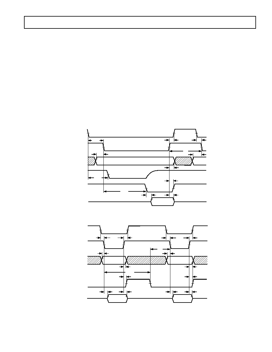
MODE 0
Figure 14 shows the timing diagram for Mode 0 operation. This
mode can only be used for microprocessors that have a WAIT
state facility, whereby a READ instruction cycle can be extended
to accommodate slow memory devices. A READ operation brings
CS and RD low, which starts a conversion. The analog multiplexer
address inputs must remain valid while
CS and RD are low. The
data bus (DB7–DB0) remains in the three-state condition until
conversion is complete. There are two converter status outputs on
the AD7824/AD7828, interrupt (
INT) and ready (RDY), which
can be used to drive the microprocessor READY/WAIT input.
The RDY is an open-drain output (no internal pull-up device) that
goes low on the falling edge of
CS and goes high impedance at the
end of conversion when the 8-bit conversion result appears on the
data outputs. If the RDY status is not required, the external
pull-up resistor can be omitted and the RDY output tied to GND.
The
INT goes low when conversion is complete and returns high
on the rising edge of
CS or RD.
MODE 1
Mode 1 operation is designed for applications where the micropro-
cessor is not forced into a WAIT state. A READ operation takes
CS and RD low, which triggers a conversion (see Figure 15). The
multiplexer address inputs are latched on the rising edge of
RD.
Data from the previous conversion is read from the three-state
data outputs (DB7–DB0). This data may be disregarded if not
required. Note that the RDY output (open drain output) does
not provide any status information in this mode and must be
connected to GND. At the end of conversion,
INT goes low. A
second READ operation is required to access the new conversion
result. This READ operation latches a new address into the multi-
plexer inputs and starts another conversion.
INT returns high at the
end of the second READ operation, when
CS or RD returns high.
A delay of 2.5
s must be allowed between READ operations.
CS
RD
ANALOG
CHANNEL
ADDRESS
RDY
INT
DATA
tCSS
tAS
tRDY
tCRD
tACC2
tDH
tINTH
tAH
tAS
tP
tCSS
tCSH
ADDRESS
VALID
ADDRESS
VALID
DATA
VALID
HIGH IMPEDANCE
Figure 14. Mode 0 Timing Diagram
CS
RD
ANALOG
CHANNEL
ADDRESS
INT
DATA
tCSS
tAS
ADDRESS
VALID
OLD
VALID
ADDRESS
VALID
NEW
VALID
tCSH
tAH
tRD
tCRD
tINTH
tACC1
tDH
tACC1
tDH
tINTH
tAH
tAS
tP
tCSS
tRD
tCSH
Figure 15. Mode 1 Timing Diagram
相关PDF资料 |
PDF描述 |
|---|---|
| AD7492BRUZ-5 | IC ADC 12BIT REF/CLOCK 24TSSOP |
| ADM3311EACPZ-REEL | IC TXRX RS-232 3:5 2.7V 32LFCSP |
| ADM3491ARU-1REEL | IC TXRX RS-485 HS 3.3V 16TSSOP |
| MS3112E14-19P | CONN RECEPT 19POS W/PINS SOLDER |
| VE-26M-CU-F2 | CONVERTER MOD DC/DC 10V 200W |
相关代理商/技术参数 |
参数描述 |
|---|---|
| AD7828BR-REEL | 制造商:Analog Devices 功能描述:ADC Single Semiflash 50ksps 8-bit Parallel 28-Pin SOIC W T/R 制造商:Analog Devices 功能描述:CONVERTER I.C. - Tape and Reel |
| AD7828BRS | 制造商:AD 制造商全称:Analog Devices 功能描述:LC2MOS High Speed 4- & 8-Channel 8-Bit ADCs |
| AD7828BRZ | 功能描述:IC ADC 8BIT 8CHAN HS 28SOIC RoHS:是 类别:集成电路 (IC) >> 数据采集 - 模数转换器 系列:- 其它有关文件:TSA1204 View All Specifications 标准包装:1 系列:- 位数:12 采样率(每秒):20M 数据接口:并联 转换器数目:2 功率耗散(最大):155mW 电压电源:模拟和数字 工作温度:-40°C ~ 85°C 安装类型:表面贴装 封装/外壳:48-TQFP 供应商设备封装:48-TQFP(7x7) 包装:Digi-Reel® 输入数目和类型:4 个单端,单极;2 个差分,单极 产品目录页面:1156 (CN2011-ZH PDF) 其它名称:497-5435-6 |
| AD7828BRZ-REEL | 功能描述:IC ADC 8BIT 8CHAN HS 28SOIC RoHS:是 类别:集成电路 (IC) >> 数据采集 - 模数转换器 系列:- 标准包装:1,000 系列:- 位数:12 采样率(每秒):300k 数据接口:并联 转换器数目:1 功率耗散(最大):75mW 电压电源:单电源 工作温度:0°C ~ 70°C 安装类型:表面贴装 封装/外壳:24-SOIC(0.295",7.50mm 宽) 供应商设备封装:24-SOIC 包装:带卷 (TR) 输入数目和类型:1 个单端,单极;1 个单端,双极 |
| AD7828CQ | 功能描述:IC ADC 8BIT 8CH HS 28-CDIP RoHS:否 类别:集成电路 (IC) >> 数据采集 - 模数转换器 系列:- 标准包装:1 系列:- 位数:14 采样率(每秒):83k 数据接口:串行,并联 转换器数目:1 功率耗散(最大):95mW 电压电源:双 ± 工作温度:0°C ~ 70°C 安装类型:通孔 封装/外壳:28-DIP(0.600",15.24mm) 供应商设备封装:28-PDIP 包装:管件 输入数目和类型:1 个单端,双极 |
发布紧急采购,3分钟左右您将得到回复。