参数资料
| 型号: | AD7840ARS |
| 厂商: | Analog Devices Inc |
| 文件页数: | 2/16页 |
| 文件大小: | 0K |
| 描述: | IC DAC 14BIT LOW POWER 5V 24SSOP |
| 产品培训模块: | Data Converter Fundamentals DAC Architectures |
| 标准包装: | 1 |
| 设置时间: | 2.5µs |
| 位数: | 14 |
| 数据接口: | 串行,并联 |
| 转换器数目: | 1 |
| 电压电源: | 双 ± |
| 功率耗散(最大): | 100mW |
| 工作温度: | -25°C ~ 85°C |
| 安装类型: | 表面贴装 |
| 封装/外壳: | 24-SSOP(0.209",5.30mm 宽) |
| 供应商设备封装: | 24-SSOP |
| 包装: | 管件 |
| 输出数目和类型: | 1 电压,双极 |
| 采样率(每秒): | 400k |
AD7840
REV. B
–10–
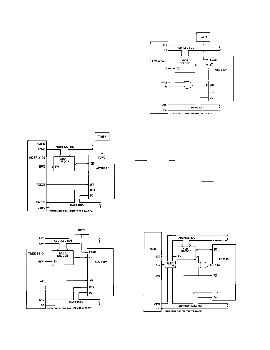
MICROPROCESSOR INTERFACING
The AD7840 logic architecture allows two interfacing options
for interfacing the part to microprocessor systems. It offers a
14-bit wide parallel format and a serial format. Fast pulse
widths and data setup times allow the AD7840 to interface
directly to most microprocessors including the DSP processors.
Suitable interfaces to various microprocessors are shown in
Figures 15 to 23.
Parallel Interfacing
Figures 15 to 17 show interfaces to the DSP processors, the
ADSP-2100, the TMS32010 and TMS32020. An external
timer controls the updating of the AD7840. Data is loaded to
the AD7840 input latch using the following instructions:
ADSP-2100: DM(DAC) = MR0
TMS32010: OUT DAC,D
TMS32020: OUT DAC,D
MR0 = ADSP-2100 MR0 Register
D = Data Memory Address
DAC = AD7840 Address
Figure 15. AD7840–ADSP-2100 Parallel Interface
Figure 16. AD7840–TMS32010 Parallel Interface
Figure 17. AD7840–TMS32020 Parallel Interface
Some applications may require that the updating of the AD7840
DAC latch be controlled by the microprocessor rather than the
external timer. One option (for double-buffered interfacing) is
to decode the AD7840 LDAC from the address bus so that a
write operation to the DAC latch (at a separate address than the
input latch) updates the output. An example of this is shown in
the 8086 interface of Figure 18. Note that connecting the
LDAC
input to the CS input will not load the DAC latch cor-
rectly since both latches cannot he transparent at the same time.
AD7840–8086 Interface
Figure 18 shows an interface between the AD7840 and the 8086
microprocessor. For this interface, the LDAC input is derived
from a decoded address. If the least significant address line, A0,
is decoded then the input latch and the DAC latch can reside at
consecutive addresses. A move instruction loads the input latch
while a second move instruction updates the DAC latch and the
AD7840 output. The move instruction to load a data word
WXYZ to the input latch is as follows:
MOV DAC,#YZWX
DAC = AD7840 Address
Figure 18. AD7840–8086 Parallel Interface
相关PDF资料 |
PDF描述 |
|---|---|
| AD7837ANZ | IC DAC 12BIT MULT DUAL 24-DIP |
| AD558JD | IC DAC 8BIT 5-15V IN MONO 16CDIP |
| LTC2755BIUP-16#TRPBF | IC DAC 16BIT CUR OUT 64-QFN |
| AD667KP | IC DAC 12BIT W/BUFF LATCH 28PLCC |
| AD7542KRZ | IC DAC 12BIT MULT CMOS 16SOIC |
相关代理商/技术参数 |
参数描述 |
|---|---|
| AD7840ARS-REEL | 功能描述:IC DAC 14BIT LOW POWER 5V 24SSOP RoHS:否 类别:集成电路 (IC) >> 数据采集 - 数模转换器 系列:- 产品培训模块:Data Converter Fundamentals DAC Architectures 标准包装:750 系列:- 设置时间:7µs 位数:16 数据接口:并联 转换器数目:1 电压电源:双 ± 功率耗散(最大):100mW 工作温度:0°C ~ 70°C 安装类型:表面贴装 封装/外壳:28-LCC(J 形引线) 供应商设备封装:28-PLCC(11.51x11.51) 包装:带卷 (TR) 输出数目和类型:1 电压,单极;1 电压,双极 采样率(每秒):143k |
| AD7840ARSZ | 功能描述:IC DAC 14BIT LOW POWER 5V 24SSOP RoHS:是 类别:集成电路 (IC) >> 数据采集 - 数模转换器 系列:- 产品培训模块:Lead (SnPb) Finish for COTS Obsolescence Mitigation Program 标准包装:50 系列:- 设置时间:4µs 位数:12 数据接口:串行 转换器数目:2 电压电源:单电源 功率耗散(最大):- 工作温度:-40°C ~ 85°C 安装类型:表面贴装 封装/外壳:8-TSSOP,8-MSOP(0.118",3.00mm 宽) 供应商设备封装:8-uMAX 包装:管件 输出数目和类型:2 电压,单极 采样率(每秒):* 产品目录页面:1398 (CN2011-ZH PDF) |
| AD7840ARSZ-REEL | 功能描述:IC DAC 14BIT LOW POWER 5V 24SSOP RoHS:是 类别:集成电路 (IC) >> 数据采集 - 数模转换器 系列:- 产品培训模块:Data Converter Fundamentals DAC Architectures 标准包装:750 系列:- 设置时间:7µs 位数:16 数据接口:并联 转换器数目:1 电压电源:双 ± 功率耗散(最大):100mW 工作温度:0°C ~ 70°C 安装类型:表面贴装 封装/外壳:28-LCC(J 形引线) 供应商设备封装:28-PLCC(11.51x11.51) 包装:带卷 (TR) 输出数目和类型:1 电压,单极;1 电压,双极 采样率(每秒):143k |
| AD7840BQ | 制造商:AD 制造商全称:Analog Devices 功能描述:LC2MOS Complete 14-Bit DAC |
| AD7840CQ | 制造商:未知厂家 制造商全称:未知厂家 功能描述:14-Bit Digital-to-Analog Converter |
发布紧急采购,3分钟左右您将得到回复。