参数资料
| 型号: | AD7840ARS |
| 厂商: | Analog Devices Inc |
| 文件页数: | 4/16页 |
| 文件大小: | 0K |
| 描述: | IC DAC 14BIT LOW POWER 5V 24SSOP |
| 产品培训模块: | Data Converter Fundamentals DAC Architectures |
| 标准包装: | 1 |
| 设置时间: | 2.5µs |
| 位数: | 14 |
| 数据接口: | 串行,并联 |
| 转换器数目: | 1 |
| 电压电源: | 双 ± |
| 功率耗散(最大): | 100mW |
| 工作温度: | -25°C ~ 85°C |
| 安装类型: | 表面贴装 |
| 封装/外壳: | 24-SSOP(0.209",5.30mm 宽) |
| 供应商设备封装: | 24-SSOP |
| 包装: | 管件 |
| 输出数目和类型: | 1 电压,双极 |
| 采样率(每秒): | 400k |
AD7840
REV. B
–12–
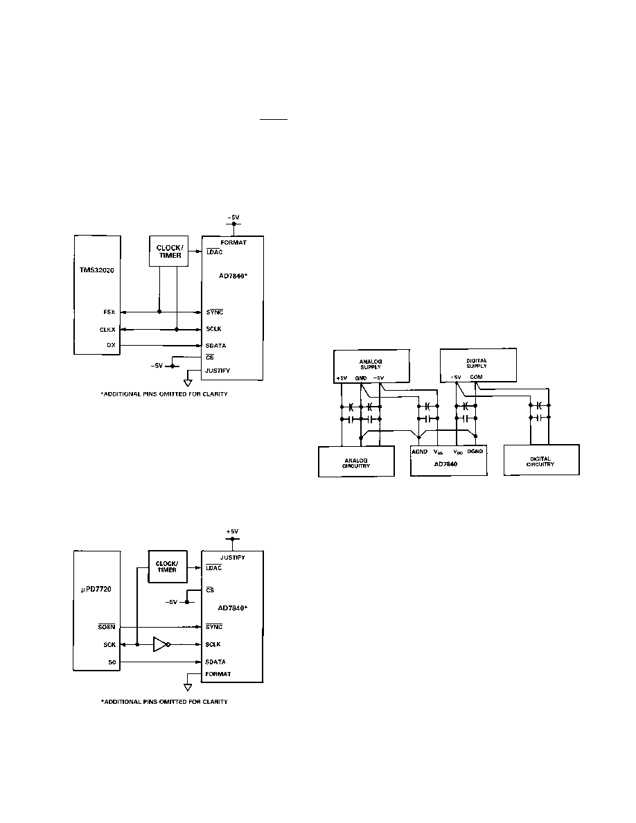
AD7840–TMS32020 Serial Interface
Figure 22 shows a serial interface between the AD7840 and the
TMS32020 DSP processor. In this interface, the CLKX and
FSX pin of the TMS32020 are generated from the clock/timer
circuitry. The same clock/timer circuitry generates the LDAC
signal of the AD7840 to synchronize the update of the output
with the serial transmission. The FSX pin of the TMS32020
must be configured as an input.
Data from the TMS32020 is valid on the falling edge of CLKX.
Once again, the FORMAT pin of the AD7840 must be tied to
+5 V while the JUSTIFY pin must be tied to DGND.
Figure 22. AD7840–TMS32020 Serial Interface
AD7840–NEC7720 Serial Interface
A serial interface between the AD7840 and the NEC7720 is
shown in Figure 23. The serial clock must be inverted before
being applied to the AD7840 SCLK input because data from
the processor is valid on the rising edge of SCK.
The NEC7720 is programmed for the LSB to be the first bit in
the serial data stream. Therefore, the AD7840 is set up with the
FORMAT pin tied to DGND and the JUSTIFY pin tied to +5 V.
Figure 23. AD7840–NEC7720 Serial Interface
APPLYING THE AD7840
Good printed circuit board layout is as important as the overall
circuit design itself in achieving high speed converter perfor-
mance. The AD7840 works on an LSB size of 366
V. There-
fore, the designer must be conscious of minimizing noise in both
the converter itself and in the surrounding circuitry. Switching
mode power supplies are not recommended as the switching
spikes can feed through to the on-chip amplifier. Other causes
of concern are ground loops and digital feedthrough from mi-
croprocessors. These are factors which influence any high per-
formance converter, and a proper PCB layout which minimizes
these effects is essential for best performance.
LAYOUT HINTS
Ensure that the layout for the printed circuit board has the digi-
tal and analog lines separated as much as possible. Take care
not to run any digital track alongside an analog signal track. Es-
tablish a single point analog ground (star ground) separate from
the logic system ground. Place this star ground as close as pos-
sible to the AD7840 as shown in Figure 24. Connect all analog
grounds to this star ground and also connect the AD7840
DGND pin to this ground. Do not connect any other digital
grounds to this analog ground point.
Figure 24. Power Supply Grounding Practice
Low impedance analog and digital power supply common re-
turns are essential to low noise operation of high performance
converters. Therefore, the foil width for these tracks should be
kept as wide as possible. The use of ground planes minimizes
impedance paths and also guards the analog circuitry from digi-
tal noise. The circuit layouts of Figures 27 and 28 have both
analog and digital ground planes which are kept separated and
only joined at the star ground close to the AD7840.
NOISE
Keep the signal leads on the VOUT signal and the signal return
leads to AGND as short as possible to minimize noise coupling.
In applications where this is not possible, use a shielded cable
between the DAC output and its destination. Reduce the
ground circuit impedance as much as possible since any poten-
tial difference in grounds between the DAC and its destination
device appears as an error voltage in series with the DAC output.
相关PDF资料 |
PDF描述 |
|---|---|
| AD7837ANZ | IC DAC 12BIT MULT DUAL 24-DIP |
| AD558JD | IC DAC 8BIT 5-15V IN MONO 16CDIP |
| LTC2755BIUP-16#TRPBF | IC DAC 16BIT CUR OUT 64-QFN |
| AD667KP | IC DAC 12BIT W/BUFF LATCH 28PLCC |
| AD7542KRZ | IC DAC 12BIT MULT CMOS 16SOIC |
相关代理商/技术参数 |
参数描述 |
|---|---|
| AD7840ARS-REEL | 功能描述:IC DAC 14BIT LOW POWER 5V 24SSOP RoHS:否 类别:集成电路 (IC) >> 数据采集 - 数模转换器 系列:- 产品培训模块:Data Converter Fundamentals DAC Architectures 标准包装:750 系列:- 设置时间:7µs 位数:16 数据接口:并联 转换器数目:1 电压电源:双 ± 功率耗散(最大):100mW 工作温度:0°C ~ 70°C 安装类型:表面贴装 封装/外壳:28-LCC(J 形引线) 供应商设备封装:28-PLCC(11.51x11.51) 包装:带卷 (TR) 输出数目和类型:1 电压,单极;1 电压,双极 采样率(每秒):143k |
| AD7840ARSZ | 功能描述:IC DAC 14BIT LOW POWER 5V 24SSOP RoHS:是 类别:集成电路 (IC) >> 数据采集 - 数模转换器 系列:- 产品培训模块:Lead (SnPb) Finish for COTS Obsolescence Mitigation Program 标准包装:50 系列:- 设置时间:4µs 位数:12 数据接口:串行 转换器数目:2 电压电源:单电源 功率耗散(最大):- 工作温度:-40°C ~ 85°C 安装类型:表面贴装 封装/外壳:8-TSSOP,8-MSOP(0.118",3.00mm 宽) 供应商设备封装:8-uMAX 包装:管件 输出数目和类型:2 电压,单极 采样率(每秒):* 产品目录页面:1398 (CN2011-ZH PDF) |
| AD7840ARSZ-REEL | 功能描述:IC DAC 14BIT LOW POWER 5V 24SSOP RoHS:是 类别:集成电路 (IC) >> 数据采集 - 数模转换器 系列:- 产品培训模块:Data Converter Fundamentals DAC Architectures 标准包装:750 系列:- 设置时间:7µs 位数:16 数据接口:并联 转换器数目:1 电压电源:双 ± 功率耗散(最大):100mW 工作温度:0°C ~ 70°C 安装类型:表面贴装 封装/外壳:28-LCC(J 形引线) 供应商设备封装:28-PLCC(11.51x11.51) 包装:带卷 (TR) 输出数目和类型:1 电压,单极;1 电压,双极 采样率(每秒):143k |
| AD7840BQ | 制造商:AD 制造商全称:Analog Devices 功能描述:LC2MOS Complete 14-Bit DAC |
| AD7840CQ | 制造商:未知厂家 制造商全称:未知厂家 功能描述:14-Bit Digital-to-Analog Converter |
发布紧急采购,3分钟左右您将得到回复。