参数资料
| 型号: | AD7841BSZ |
| 厂商: | Analog Devices Inc |
| 文件页数: | 12/13页 |
| 文件大小: | 0K |
| 描述: | IC DAC 14BIT OCTAL V-OUT 44-MQFP |
| 产品培训模块: | Data Converter Fundamentals DAC Architectures |
| 标准包装: | 1 |
| 设置时间: | 31µs |
| 位数: | 14 |
| 数据接口: | 并联 |
| 转换器数目: | 8 |
| 电压电源: | 模拟和数字,双 ± |
| 功率耗散(最大): | 303mW |
| 工作温度: | -40°C ~ 85°C |
| 安装类型: | 表面贴装 |
| 封装/外壳: | 44-QFP |
| 供应商设备封装: | 44-MQFP(10x10) |
| 包装: | 托盘 |
| 输出数目和类型: | 8 电压,单极;8 电压,双极 |
| 采样率(每秒): | 32k |
| 产品目录页面: | 785 (CN2011-ZH PDF) |
| 配用: | EVAL-AD7841EBZ-ND - BOARD EVAL FOR AD7841 |
AD7841
–8–
Unipolar Configuration
Figure 2 shows the AD7841 in the unipolar binary circuit
configuration. The VREF(+) input of the DAC is driven by the
AD586, a 5 V reference. VREF(–) is tied to ground. Table II
gives the code table for unipolar operation of the AD7841.
Other suitable references include the REF02, a precision 5 V
reference, and the REF195, a low dropout, micropower preci-
sion 5 V reference.
AD7841*
VDD
VCC
VREF(+)
VOUT
DUTGND
GND
VSS
VREF(–)
SIGNAL
GND
–15V
VOUT
(0 TO +10V)
+5V
+15V
AD586
R1
10k
2
6
5
4
8
C1
1 F
SIGNAL
GND
*ADDITIONAL PINS OMITTED FOR CLARITY
Figure 2. Unipolar 10 V Operation
Offset and gain may be adjusted in Figure 2 as follows: To
adjust offset, disconnect the VREF(–) input from 0 V, load the
DAC with all 0s and adjust the VREF(–) voltage until VOUT = 0 V.
For gain adjustment, the AD7841 should be loaded with all 1s
and R1 adjusted until VOUT = 2 VREF(+) – 1 LSB = 10 V(16383/
16384) = 9.99939 V.
Many circuits will not require these offset and gain adjustments.
In these circuits R1 can be omitted. Pin 5 of the AD586 may be
left open circuit and Pin 2 (VREF(–)) of the AD7841 tied to 0 V.
Table II. Code Table for Unipolar Operation
Binary Number in DAC Register
Analog Output
MSB
LSB
(VOUT)
11
1111
2 VREF (16383/16384) V
10
0000
2 VREF (8192/16384) V
01
1111
2 VREF (8191/16384) V
00
0000
0001
2 VREF (1/16384) V
00
0000
0 V
NOTES
V= VREF(+); VREF(–) = 0 V for unipolar operation.
For VREF(+) = 5 V, 1 LSB = 10 V/2
14 = 10 V/16384 = 610
V.
Bipolar Configuration
Figure 3 shows the AD7841 set up for
± 10 V operation. The
AD588 provides precision
±5 V tracking outputs that are fed to
the VREF(+) and VREF(–) inputs of the AD7841. The code table
for bipolar operation of the AD7841 is shown in Table III.
In Figure 3, full-scale and bipolar zero adjustments are provided
by varying the gain and balance on the AD588. R2 varies the
gain on the AD588 while R3 adjusts the offset of both the +5 V
and –5 V outputs together with respect to ground.
For bipolar-zero adjustment, the DAC is loaded with
1000... 0000 and R3 is adjusted until VOUT = 0 V. Full scale
is adjusted by loading the DAC with all 1s and adjusting R2
until VOUT = 10(8191/8192) V = 9.99878 V.
When bipolar-zero and full-scale adjustment are not needed, R2
and R3 can be omitted. Pin 12 on the AD588 should be con-
nected to Pin 11 and Pin 5 should be left floating.
AD7841*
VDD
VCC
VREF(+)
VOUT
DUTGND
GND
VSS
VREF(–)
SIGNAL
GND
–15V
VOUT
(–10V TO +10V)
+5V
+15V
*ADDITIONAL PINS OMITTED FOR CLARITY
R1
39k
C1
1 F
R2
100k
R3
100k
AD588
46
2
3
1
14
15
16
7
9
5
10
11
12
8 13
Figure 3. Bipolar
±10 V Operation
Table III. Code Table for Bipolar Operation
Binary Number in DAC
Register
Analog Output
MSB
LSB
(VOUT)
11
1111 1111
1111
2[VREF(–) + VREF (16383/16384)] V
10
0000 0000
0001
2[VREF(–) + VREF (8193/16384)] V
10
0000 0000
0000
2[VREF(–) + VREF (8192/16384)] V
01
1111 1111
1111
2[VREF(–) + VREF (8191/16384)] V
00
0000 0000
0001
2[VREF(–) + VREF (1/16384)] V
00
0000 0000
0000
2[VREF(–)] V
NOTES
VREF = (VREF(+) – VREF(–)).
For VREF(+) = +5 V, and VREF(–) = –5 V, VREF = 10 V, 1 LSB = 2 VREF V/2
14 =
20 V/16384 = 1.22 mV.
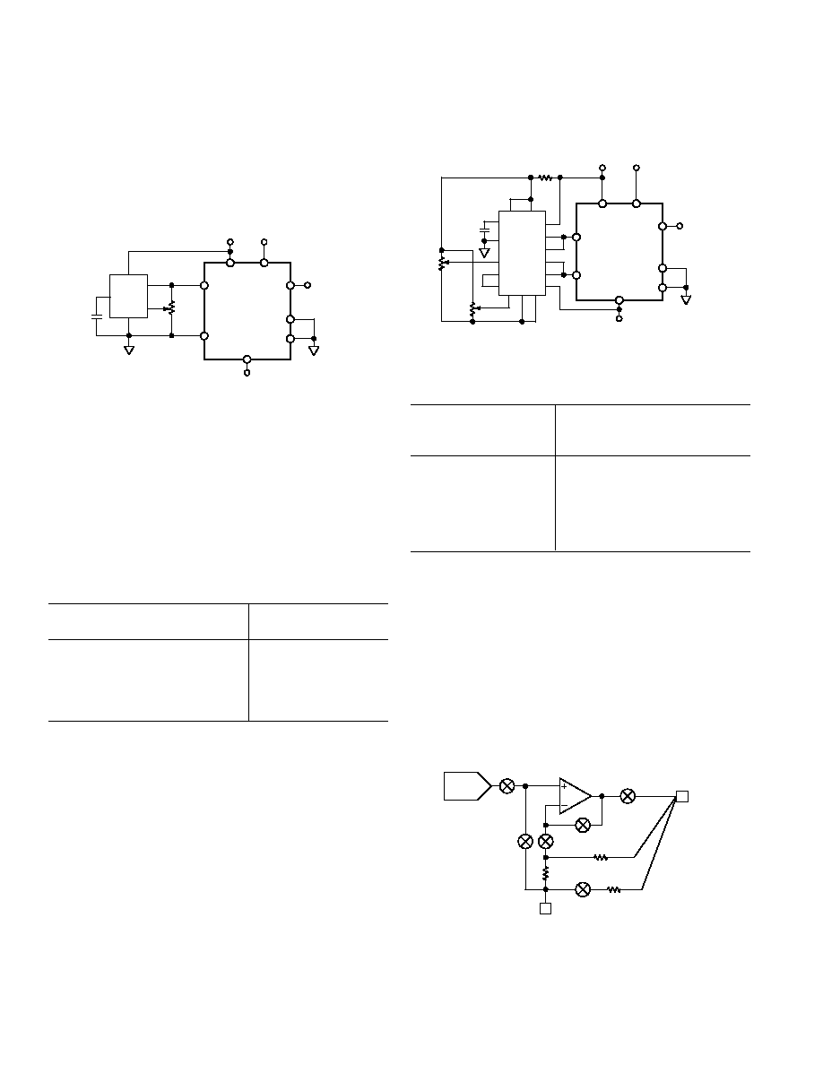
CONTROLLED POWER-ON OF THE OUTPUT STAGE
A block diagram of the output stage of the AD7841 is shown in
Figure 4. It is capable of driving a load of 5 k
in parallel with
50 pF. G1 to G6 are transmission gates used to control the
power on voltage present at VOUT. On power up G1 and G2 are
also used in conjunction with the
CLR input to set V
OUT to the
user defined voltage present at the DUTGND pin. When
CLR
is taken back high, the DAC outputs reflect the data in the
DAC registers.
G1
G2
G4
G3
G6
G5
DUTGND
VOUT
R
R = 60k
14k
DAC
Figure 4. Block Diagram of AD7841 Output Stage
REV. B
相关PDF资料 |
PDF描述 |
|---|---|
| AD569JPZ | IC DAC 16BIT MONO NON-LIN 28PLCC |
| AD9146BCPZ | IC DAC 16BIT SRL DUAL 48LFCSP |
| GTC02R-36-5P | CONN RCPT 4POS BOX MNT W/PINS |
| VE-2TY-MX-F2 | CONVERTER MOD DC/DC 3.3V 49.5W |
| MS27508E24B4PC | CONN RCPT 56POS BOX MNT W/PINS |
相关代理商/技术参数 |
参数描述 |
|---|---|
| AD7841BSZ | 制造商:Analog Devices 功能描述:IC 14-BIT DAC |
| AD7841BSZ-REEL | 功能描述:IC DAC 14BIT OCTAL VOUT 44-MQFP RoHS:是 类别:集成电路 (IC) >> 数据采集 - 数模转换器 系列:- 产品培训模块:Lead (SnPb) Finish for COTS Obsolescence Mitigation Program 标准包装:1,000 系列:- 设置时间:1µs 位数:8 数据接口:串行 转换器数目:8 电压电源:双 ± 功率耗散(最大):941mW 工作温度:0°C ~ 70°C 安装类型:表面贴装 封装/外壳:24-SOIC(0.295",7.50mm 宽) 供应商设备封装:24-SOIC W 包装:带卷 (TR) 输出数目和类型:8 电压,单极 采样率(每秒):* |
| AD7843 | 制造商:AD 制造商全称:Analog Devices 功能描述:Touch Screen Digitizer |
| AD7843ARQ | 制造商:Analog Devices 功能描述:TOUCH SCREEN DIGITIZER 制造商:Rochester Electronics LLC 功能描述:2.7V 12-BIT TOUCH SCREN DIGITIZER I.C. - Bulk 制造商:Analog Devices 功能描述:IC 12-BIT ADC |
| AD7843ARQ-REEL | 制造商:Analog Devices 功能描述:TOUCH SCREEN DIGITIZER 制造商:Rochester Electronics LLC 功能描述:2.7V 12-BIT TOUCH SCREN DIGITIZER I.C. - Tape and Reel |
发布紧急采购,3分钟左右您将得到回复。