- 您现在的位置:买卖IC网 > PDF目录9713 > AD7843ARUZ-REEL7 (Analog Devices Inc)IC ADC 12BIT TOUCHSCREEN 16TSSOP PDF资料下载
参数资料
| 型号: | AD7843ARUZ-REEL7 |
| 厂商: | Analog Devices Inc |
| 文件页数: | 5/21页 |
| 文件大小: | 0K |
| 描述: | IC ADC 12BIT TOUCHSCREEN 16TSSOP |
| 标准包装: | 1,000 |
| 类型: | 电阻 |
| 触摸面板接口: | 4 线 |
| 输入数/键: | 1 TSC |
| 分辨率(位): | 12 b |
| 评估套件: | 可供 |
| 数据接口: | 串行 |
| 数据速率/采样率 (SPS,BPS): | 125k |
| 电压基准: | 外部 |
| 电源电压: | 2.2 V ~ 5.25 V |
| 工作温度: | -40°C ~ 85°C |
| 安装类型: | 表面贴装 |
| 封装/外壳: | 16-TSSOP(0.173",4.40mm 宽) |
| 供应商设备封装: | 16-TSSOP |
| 包装: | 带卷 (TR) |
| 配用: | EVAL-AD7843EBZ-ND - BOARD EVAL FOR AD7843 |
AD7843
Rev. B | Page 12 of 20
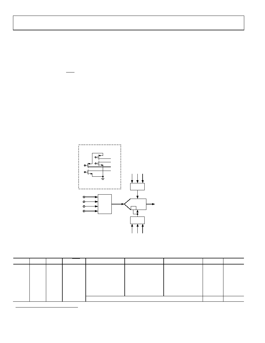
ANALOG INPUT
Figure 19 shows an equivalent circuit of the analog input
structure of the AD7843, which contains a block diagram of the
input multiplexer, the differential input of the ADC, and the
differential reference.
Table 5 shows the multiplexer address corresponding to each
analog input, both for the SER/DFR bit in the control register
set high and low. The control bits are provided serially to the
device via the DIN pin. For more information on the control
register, see the Control Register section.
When the converter enters hold mode, the voltage difference
between the +IN and IN inputs (see Figure 19) is captured on
the internal capacitor array. The input current on the analog
inputs depends on the conversion rate of the device. During the
sample period, the source must charge the internal sampling
capacitor (typically 37 pF). Once the capacitor is fully charged,
there is no further input current. The rate of charge transfer
from the analog source to the converter is a function of
conversion rate.
Acquisition Time
The track-and-hold amplifier enters tracking mode on the
falling edge of the fifth DCLK after the START bit us detected
(see Figure 24). The time required for the track-and-hold
amplifier to acquire an input signal depends on how quickly the
37 pF input capacitance is charged. With zero source impedance
on the analog input, three DCLK cycles are always sufficient to
acquire the signal to the 12-bit level. With a source impedance
RIN on the analog input, the actual acquisition time required is
calculated using the formula:
(
)
pF
37
100
4
.
8
×
+
×
=
IN
ACQ
R
t
where RIN is the source impedance of the input signal and 100
and 37 pF is the input RC value. Depending on the frequency of
DCLK used, three DCLK cycles may or may not be sufficient to
acquire the analog input signal with various source impedance
values.
02144-B
-019
VCC
X+
X+ Y+
REF
EXT
X– Y– GND
X+
Y+
IN3
IN4
X–
Y+
Y–
ON-CHIP SWITCHES
4-TO-1
MUX
3-TO-1
MUX
3-TO-1
MUX
IN+
IN– REF–
REF+
ADC CORE
DATA OUT
Figure 19. Equivalent Analog Input Circuit
Table 5. Analog Input, Reference, and Touch Screen Control
A21
A11
A01
SER/DFR
Analog Input
X Switches
Y Switches
+REF2
–REF2
0
1
X+
OFF
ON
VREF
GND
0
1
0
1
IN3
OFF
VREF
GND
1
0
1
Y+
ON
OFF
VREF
GND
1
0
1
IN4
OFF
VREF
GND
0
1
0
X+
OFF
ON
Y+
Y
1
0
1
0
Y+
ON
OFF
X+
X
1
0
Outputs Identity Code, 1000 0000 0000
1 All remaining configurations are invalid addresses.
2 Internal node not directly accessible by the user.
相关PDF资料 |
PDF描述 |
|---|---|
| VE-24F-IW-B1 | CONVERTER MOD DC/DC 72V 100W |
| VI-JWK-MX-F1 | CONVERTER MOD DC/DC 40V 75W |
| VE-24B-IW-B1 | CONVERTER MOD DC/DC 95V 100W |
| VI-BTM-IV-B1 | CONVERTER MOD DC/DC 10V 150W |
| AD7843ARQZ-REEL7 | IC ADC 12BIT TOUCHSCREEN 16-QSOP |
相关代理商/技术参数 |
参数描述 |
|---|---|
| AD7845 | 制造商:AD 制造商全称:Analog Devices 功能描述:LC2MOS Complete 12-Bit Multiplying DAC |
| AD7845AQ | 功能描述:IC DAC 12BIT MULT LC2MOS 24-CDIP RoHS:否 类别:集成电路 (IC) >> 数据采集 - 数模转换器 系列:- 产品培训模块:Data Converter Fundamentals DAC Architectures 标准包装:750 系列:- 设置时间:7µs 位数:16 数据接口:并联 转换器数目:1 电压电源:双 ± 功率耗散(最大):100mW 工作温度:0°C ~ 70°C 安装类型:表面贴装 封装/外壳:28-LCC(J 形引线) 供应商设备封装:28-PLCC(11.51x11.51) 包装:带卷 (TR) 输出数目和类型:1 电压,单极;1 电压,双极 采样率(每秒):143k |
| AD7845AR | 制造商:Rochester Electronics LLC 功能描述:12-BIT PARALLEL VOUT DAC, IC - Bulk 制造商:Analog Devices 功能描述: |
| AD7845ARZ | 功能描述:IC DAC 12BIT MULT LC2MOS 24SOIC RoHS:是 类别:集成电路 (IC) >> 数据采集 - 数模转换器 系列:- 产品培训模块:Data Converter Fundamentals DAC Architectures 标准包装:750 系列:- 设置时间:7µs 位数:16 数据接口:并联 转换器数目:1 电压电源:双 ± 功率耗散(最大):100mW 工作温度:0°C ~ 70°C 安装类型:表面贴装 封装/外壳:28-LCC(J 形引线) 供应商设备封装:28-PLCC(11.51x11.51) 包装:带卷 (TR) 输出数目和类型:1 电压,单极;1 电压,双极 采样率(每秒):143k |
| AD7845BQ | 功能描述:IC DAC 12BIT MULT LC2MOS 24-CDIP RoHS:否 类别:集成电路 (IC) >> 数据采集 - 数模转换器 系列:- 产品培训模块:Data Converter Fundamentals DAC Architectures 标准包装:750 系列:- 设置时间:7µs 位数:16 数据接口:并联 转换器数目:1 电压电源:双 ± 功率耗散(最大):100mW 工作温度:0°C ~ 70°C 安装类型:表面贴装 封装/外壳:28-LCC(J 形引线) 供应商设备封装:28-PLCC(11.51x11.51) 包装:带卷 (TR) 输出数目和类型:1 电压,单极;1 电压,双极 采样率(每秒):143k |
发布紧急采购,3分钟左右您将得到回复。